Method and program product for designing hierarchical circuit for quiescent current testing and circuit produced thereby

Inactive Publication Date: 2005-03-15
SIEMENS PROD LIFECYCLE MANAGEMENT SOFTWARE INC
View PDF17 Cites 15 Cited by
  • Summary
  • Abstract
  • Description
  • Claims
  • Application Information

AI Technical Summary

Benefits of technology

The present invention provides a hierarchical design method for integrated circuits to be tested using quiescent current monitoring and a circuit designed according to the method. The method allows the state of the entire circuit to be set in a repeatable and predictable manner which avoids the need to analyze the entire circuit at once. The circuit is divided into hierarc

Problems solved by technology
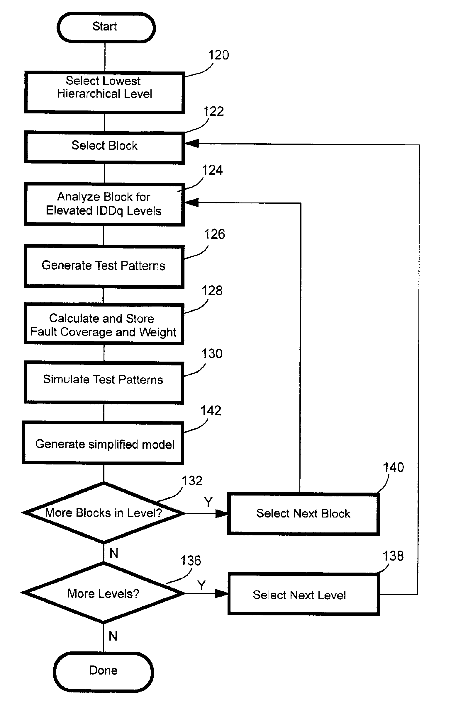
There is one type of test that does not readily lend itself to this hierarchical design methodology.
To date, the quiescent current test, and t

Method used


Image

  • Method and program product for designing hierarchical circuit for quiescent current testing and circuit produced thereby
  • Method and program product for designing hierarchical circuit for quiescent current testing and circuit produced thereby
  • Method and program product for designing hierarchical circuit for quiescent current testing and circuit produced thereby

Examples


Embodiment Construction

In the following detailed description, numerous specific details are set forth in order to provide a thorough understanding of the present invention, However, it will be understood by those skilled in the art that the present invention may be practiced without these specific details. In other instances, well known methods, procedures, components and circuits have not been described in detail so as not to obscure aspects of the present invention.

As is known in the art, integrated circuit devices are typically designed and fabricated using one or more computer data files that define the layout of the circuit arrangements of the devices. The files are typically generated by a design tool and are subsequently used during manufacturing to create the layout masks that define the circuit arrangements applied to a semiconductor wafer. Typically, the programs are provided in a predefined format using a hardware description language (HDL) such as VHDL, verilog, EDIF, etc. While the invention ...


PUM


Abstract

A method of designing integrated circuits having an hierarchical structure for quiescent current testing, and the circuit which results therefrom is disclosed. The method comprises analyzing each of one or more selected hierarchical blocks independently of other selected blocks identify any circuit states of each block which could result in elevated quiescent current levels during quiescent current testing of the circuit, the analysis beginning with blocks at a lowest level of hierarchy and proceeding in sequence through each level of design hierarchy to a highest level of hierarchy containing a top-level block; and calculating a fault coverage for each selected block.

Description

The present invention relates, in general to the design and testing of integrated circuits and, more specifically, to a method and a program product for designing circuits in a manner to facilitate quiescent current (IDDq) testing of the circuit and to a circuit designed according to the method.BACKGROUND OF THE INVENTIONThe complexity of semiconductor circuits often requires partitioning the circuit design into several core modules or blocks, generally referred to as design hierarchy. The blocks can be verified and laid out independently from each other. This design approach has been used for a long time and has several benefits, the most significant of which are to accelerate the development of the design by allowing several designers to work in parallel and to reduce the difficulty for design automation tools by avoiding the need to manipulate the description of the entire circuit at once.It has been shown recently that scan test methods can be adapted to a hierarchical design me...

Claims


Application Information

Patent Timeline
IPC IPC(8): G01R31/28G01R31/30
CPCG01R31/3012
Inventor NADEAU-DOSTIE, BENOITCOTE, JEAN-FRAN.CEDILLA.OIS
Owner SIEMENS PROD LIFECYCLE MANAGEMENT SOFTWARE INC
Why Eureka
Try Eureka