Varying feature size in resist across the chip without the artifact of "grid-snapping" from the mask writing tool

a technology of resist and feature size, applied in the field of image sensors, can solve the problems of limitation of the address grid of the mask writing tool, and achieve the effect of small spot size and variable resist feature siz

Active Publication Date: 2005-03-22
OMNIVISION TECH INC
View PDF8 Cites 0 Cited by
  • Summary
  • Abstract
  • Description
  • Claims
  • Application Information

AI Technical Summary

Benefits of technology

The present invention has the following advantages: varying the feature size in resist across the chip without the artifact of grid-snapping from the mask-writing tool; and the incremental difference in feature dimension allowed by this method is so small as to be prohibitive (i.e. very small spot size) with the current mask-writing technology.

Problems solved by technology

Such techniques, however, are subject to the limitation of the mask writing tool address grid (spot size) when determining the minimum possible critical dimension difference within a pattern.

Method used


Image

  • Varying feature size in resist across the chip without the artifact of "grid-snapping" from the mask writing tool
  • Varying feature size in resist across the chip without the artifact of "grid-snapping" from the mask writing tool
  • Varying feature size in resist across the chip without the artifact of "grid-snapping" from the mask writing tool

Examples


Embodiment Construction

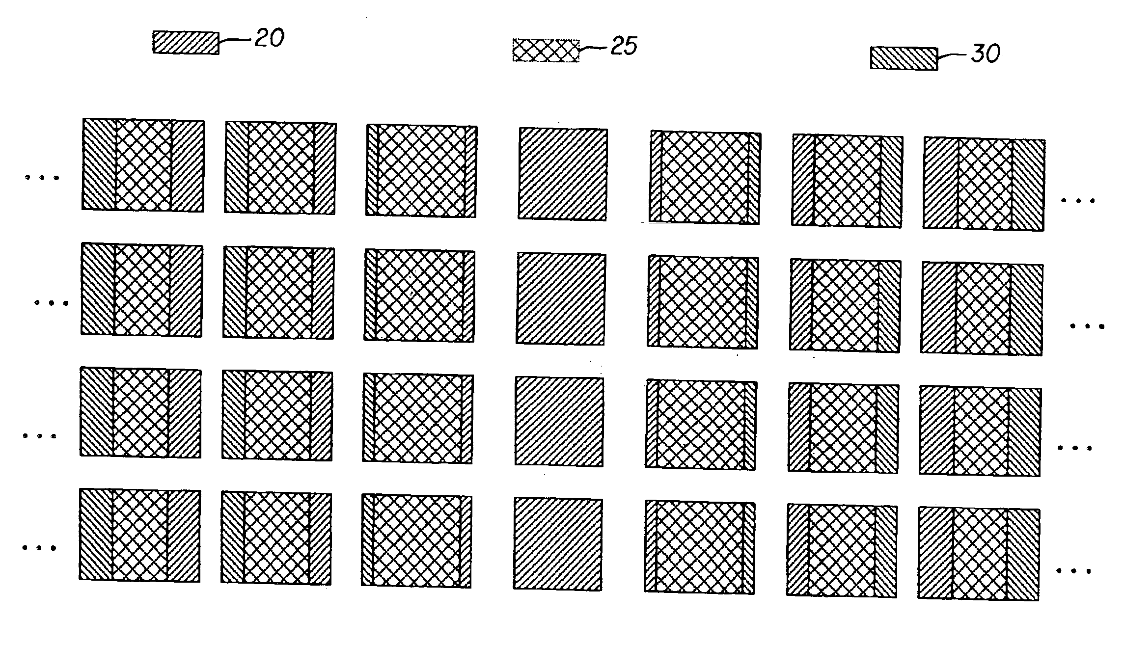
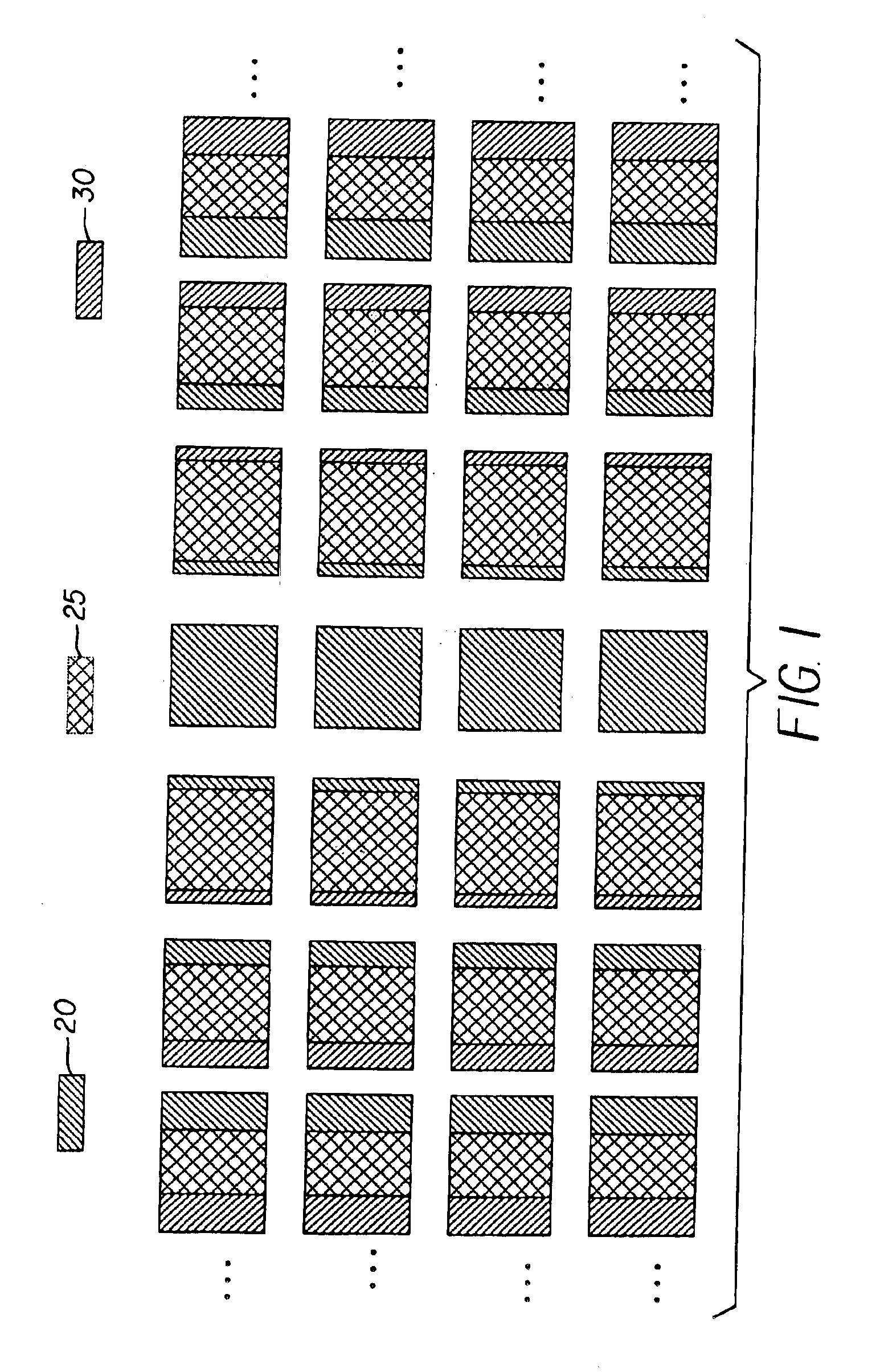
Referring to FIG. 1, there is shown a top view of a substrate of the present invention having a predetermined or systematic variation in the sizes of the apertures created across the substrate. It facilitates understanding to note that either mask writing or a stepper (both referred to hereinafter as lithography tool) is used to create the apertures. Such lithography tools are well in the art and will not be described in detail herein. The lithography tool exposes the first pattern 20 of apertures at substantially the same time across the substrate which pattern is shown in FIG. 1. The lithography tool then exposes a second pattern 30 of apertures that are mis-registered (not in exact alignment) with regard to the first pattern. The mis-registration across the substrate is such that the second pattern 30 is scaled or magnified with respect to the first pattern 20. The resulting combination of the first 20 and second 30 pattern is a series of apertures that increase in size across th...


PUM

PropertyMeasurementUnit
sizesaaaaaaaaaa
aperture sizeaaaaaaaaaa
sizeaaaaaaaaaa

Abstract

A method for creating a pattern on a substrate, the method includes the steps of imprinting a first pattern on the substrate; and imprinting a second substantially similar pattern which is mis-registered with regard to the first pattern so that the combination of the first and second patterns cause a systematic variation in a final size of defined elements across the substrate.

Description

FIELD OF THE INVENTIONThe invention relates generally to the field of image sensors and, more particularly, to apertures for such image sensors having an increasing aperture size as the apertures approach the periphery of the image sensor.BACKGROUND OF THE INVENTIONSystematic variations in critical dimension feature size of lithographically defined images may sometimes be required to compensate for process variability in the semiconductor industry. Currently, the prior art addresses only the elimination of systematic variation such as U.S. Pat. No. 6,331,711. Such techniques, however, are subject to the limitation of the mask writing tool address grid (spot size) when determining the minimum possible critical dimension difference within a pattern.Consequently, a need exists for a method which permits a virtually continuous variation of feature size by superimposing two exposures that are identical except for their distortion terms; that is to say magnification, rotation, translation...

Claims


Application Information

Patent Timeline
Patent Type & Authority Patents(United States)
IPC IPC(8): G03F7/00G03F1/14G03F7/20
CPCB82Y10/00G03F1/144G03F7/70466G03F7/203G03F7/0005G03F7/0035G03F1/70
Inventor FABINSKI, ROBERT P.SUMMA, JOSEPH R.
Owner OMNIVISION TECH INC
Why Eureka
Try Eureka