Method and test structures for measuring interconnect coupling capacitance in an IC chip

a technology of coupling capacitance and test structure, which is applied in the direction of resistance/reactance/impedence, instruments, measurement devices, etc., can solve the problems of chip functional failure, error induced by the mismatch between the two inverters, and is not suitable for on-wafer measurement, etc., to achieve accurate measurement of intra-layer coupling capacitance

Inactive Publication Date: 2005-03-22
WINBOND ELECTRONICS CORP
View PDF3 Cites 15 Cited by
  • Summary
  • Abstract
  • Description
  • Claims
  • Application Information

AI Technical Summary

Benefits of technology

The purpose of the invention is to provide new test structures and a new measurement method employing the test structures for accurately measuring intra-layer coupling capacitance between interconnect lines of an integrated circuit structure formed on an IC chip.
In conclusion, the new structures and method of the invention can improve the disadvantages of previous methods and test structures in the art such as those mentioned in the background section and satisfy the requirements of reduced mismatch effect, small test structure size, simple measurement procedure, and high accuracy in intra-layer coupling capacitance extraction.

Problems solved by technology

In addition, as interconnection becomes multi-layers, more complex and more close, the crosstalk coupling effect between wires becomes a source of noise in deep sub-micron analog and digital circuits, which can result in chip functional failures.
Besides, the error induced by the mismatch between the two inverters is another important issue of CBCM method.
However, this method requires three measurement steps and needs more pads to implement the test structure, thus it's not suitable for an on-wafer measurement.

Method used


Image

  • Method and test structures for measuring interconnect coupling capacitance in an IC chip
  • Method and test structures for measuring interconnect coupling capacitance in an IC chip
  • Method and test structures for measuring interconnect coupling capacitance in an IC chip

Examples


Embodiment Construction

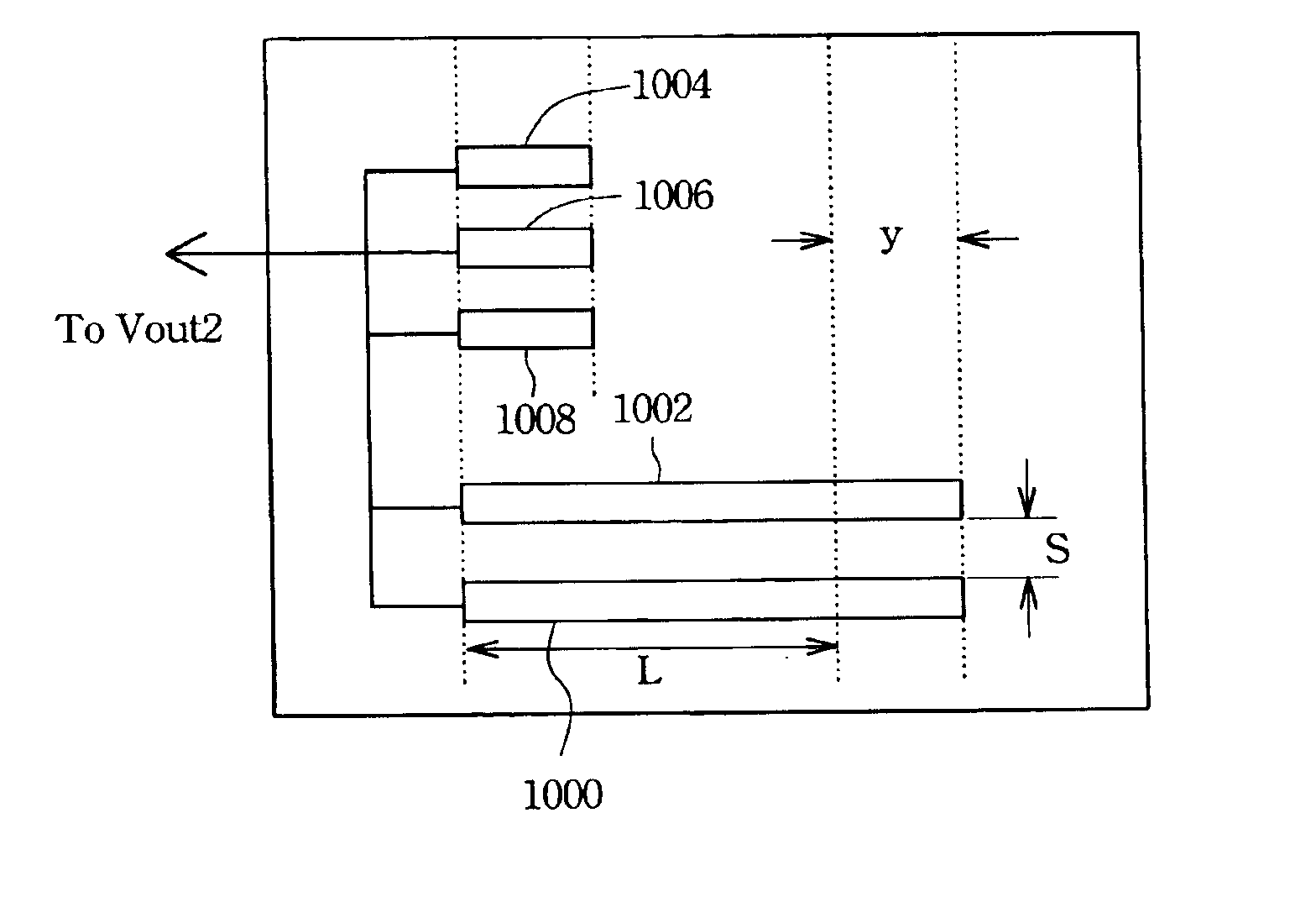
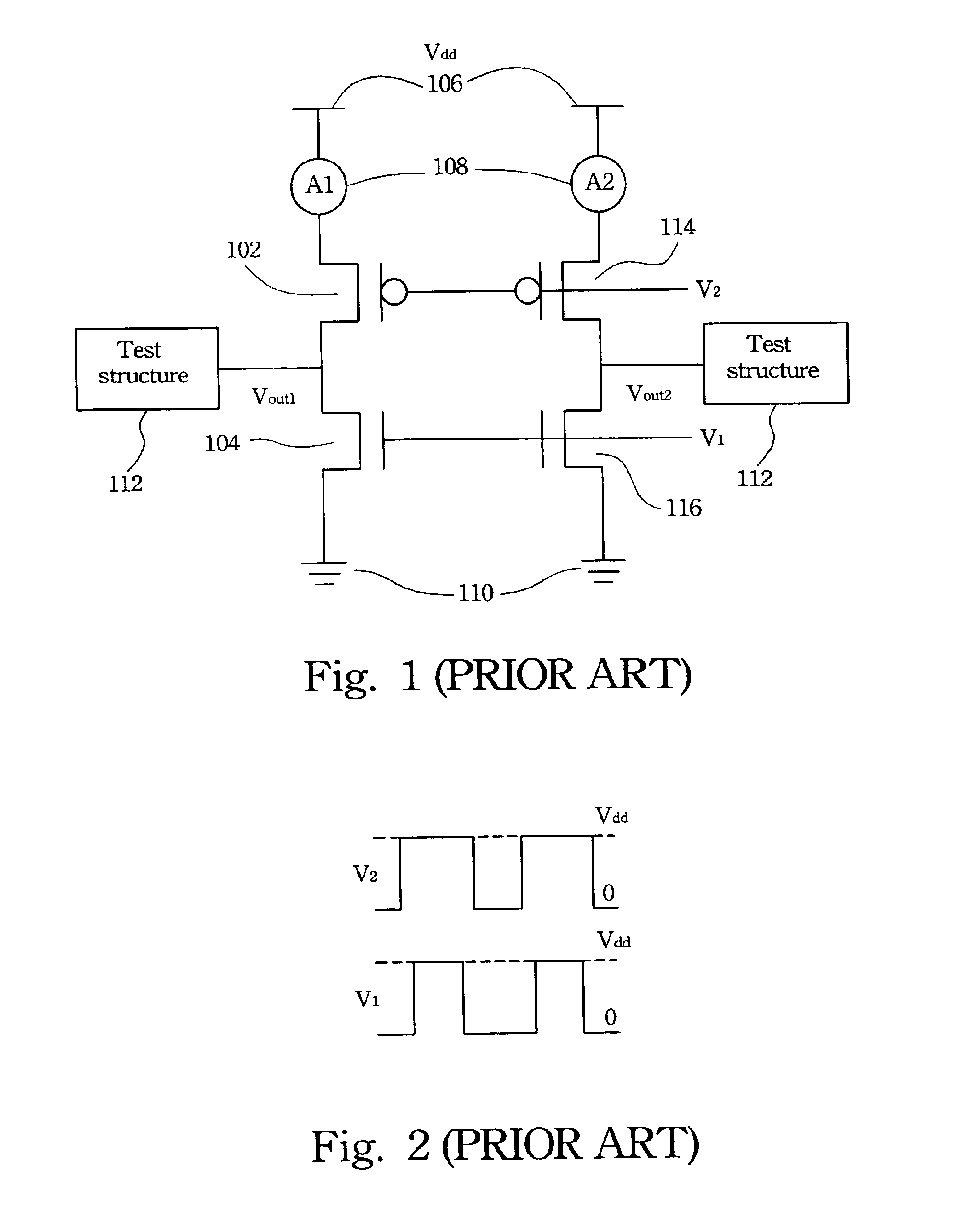
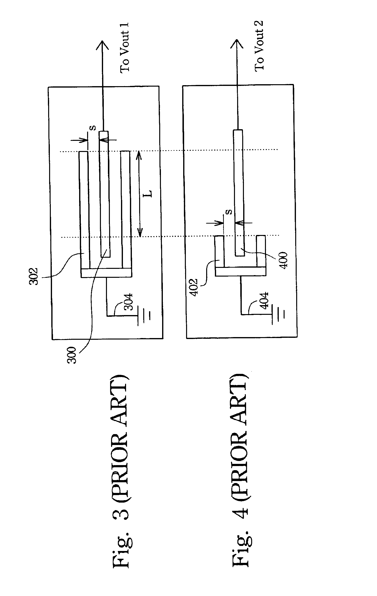
This invention proposes a new two-step measurement method and test structures for measuring the coupling capacitance between interconnect lines of an integrated circuit structure formed on an IC chip. It also adopts CBCM technique but improves the dummy test structure of J. Chen's method, and two additional test structures are used. The embodiments of the new test structures and procedures of the method are described in detail hereinafter.

The two-step measurement method is to measure a target configuration and a dummy configuration separately. The target configuration includes basically a first branch circuit and a second branch circuit, such as the two inverters in FIG. 1. The first branch circuit is the left-hand side inverter in FIG. 1 composed of the first PMOS transistor 102 and the first NMOS transistor 104. The first PMOS transistor 102 and the first NMOS transistor 104 are connected in series at the output terminal Vout1. An output terminal of the first PMOS transistor 102 (...


PUM


Abstract

Measurement method and test structures for measuring interconnect coupling capacitance in an IC chip are provided. This method employs CBCM technique. In the first step, two test structures are used to measure a target configuration in order to obtain the total capacitance C of a metal line with respect to ground including line-to-line, fringe and area components (C=2Cc+2Cf+Ca). In the second step, two other test structures are used to measure a dummy configuration in order to obtain the area and fringe capacitance Cdummy of the metal line with respect to ground including fringe and area components (Cdummy=2Cf+Ca). After the two steps, the coupling capacitance Cc between the metal line and another line can be determined according to the formula Cc=(C−Cdummy) / 2.

Description

BACKGROUND OF THE INVENTION1. Field of InventionThe present invention relates to the measurement of capacitances, and more specifically to measurement of the coupling capacitance between interconnect lines of an integrated circuit (IC) structure.2. Description of Related ArtAs transistor scaling continues, gate delay is no longer the major limit of circuit speed and instead interconnect delay dominates the circuit performance. In addition, as interconnection becomes multi-layers, more complex and more close, the crosstalk coupling effect between wires becomes a source of noise in deep sub-micron analog and digital circuits, which can result in chip functional failures. Therefore, to extract accurate interconnect parameters for circuit simulation or for circuit failure analysis is needed and important.In order to evaluate the coupling effect between interconnect lines, it's necessary to ascertain the coupling capacitances between lines. The coupling capacitance includes both intra-la...

Claims


Application Information

Patent Timeline
Patent Type & Authority Patents(United States)
IPC IPC(8): G01R31/28
CPCG01R31/2884G01R31/2853
Inventor HUANG, KAI-YECHAO, CHUAN-JANE
Owner WINBOND ELECTRONICS CORP
Why Eureka
Try Eureka