Thin gate oxide output drive

a driver and oxide technology, applied in the direction of pulse technique, oscillation generator, reliability increasing modifications, etc., can solve the problems of vlsi circuits that tend to lead in the area of size and voltage scaling, vlsi device sizes and operating voltages have decreased, and the size and voltage of vlsi devices are not easy to scal

Inactive Publication Date: 2005-03-22
IP FIRST
View PDF16 Cites 18 Cited by
  • Summary
  • Abstract
  • Description
  • Claims
  • Application Information

AI Technical Summary

Benefits of technology

A scaled output driver according to an embodiment of the present invention includes first and second scaled P-channel devices and an N-channel device. The first scaled P-channel device has a drain and a source coupled between a first node and an elevated source voltage having an elevated voltage level. The first scaled P-channel device has a gate that receives a pull-up signal that turns the first scaled P-channel device off when driven towards

Problems solved by technology

Very Large Scale Integrated (VLSI) circuits, particularly microprocessors, tend to lead in the area of size and voltage scaling.
In more recent years, VLSI device sizes and operating voltages have decreased to the extent that, in some cases, scaled P-channel devices that provide an interface to elevated voltage external devices experience gate oxide breakdown if those same elevated voltage levels are used to drive their inputs.
As a result, pulling a 0.18 micron P-channel output device up to 3.3 volts, while holding its gate at zero volts will very likely damage the gate oxide of the P-channel device.
Notwithstanding the protection afforded by output voltage scaling circuits, a conventional scaled output driver circuit experiences related problems when driving elevated voltages on a tri-state bus, such as when the P-channel dev

Method used


Image

  • Thin gate oxide output drive
  • Thin gate oxide output drive
  • Thin gate oxide output drive

Examples


Embodiment Construction

The following description is presented to enable one of ordinary skill in the art to make and use the present invention as provided within the context of a particular application and its requirements. Various modifications to the preferred embodiment will, however, be apparent to one skilled in the art, and the general principles defined herein may be applied to other embodiments. Therefore, the present invention is not intended to be limited to the particular embodiments shown and described herein, but is to be accorded the widest scope consistent with the principles and novel features herein disclosed.

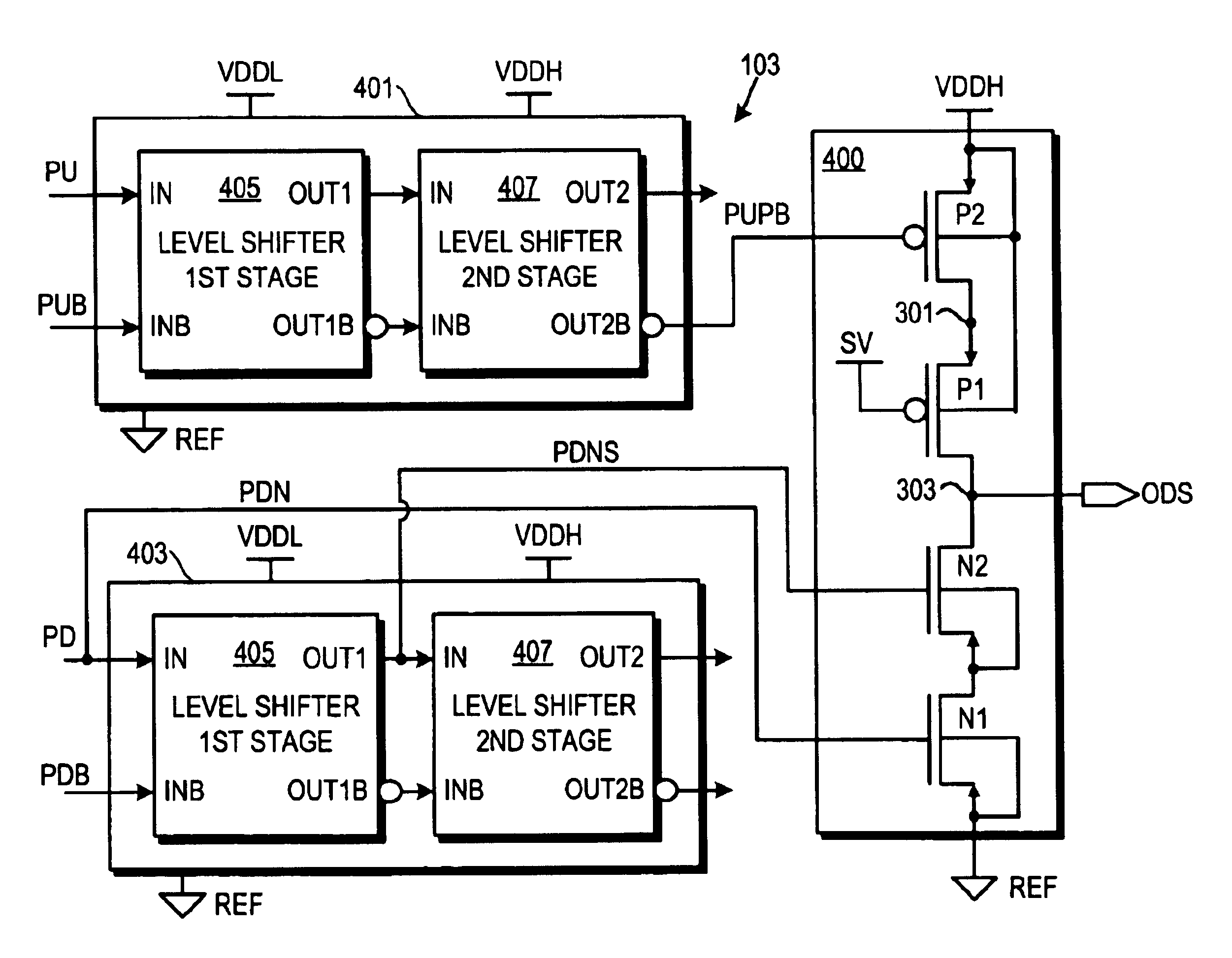
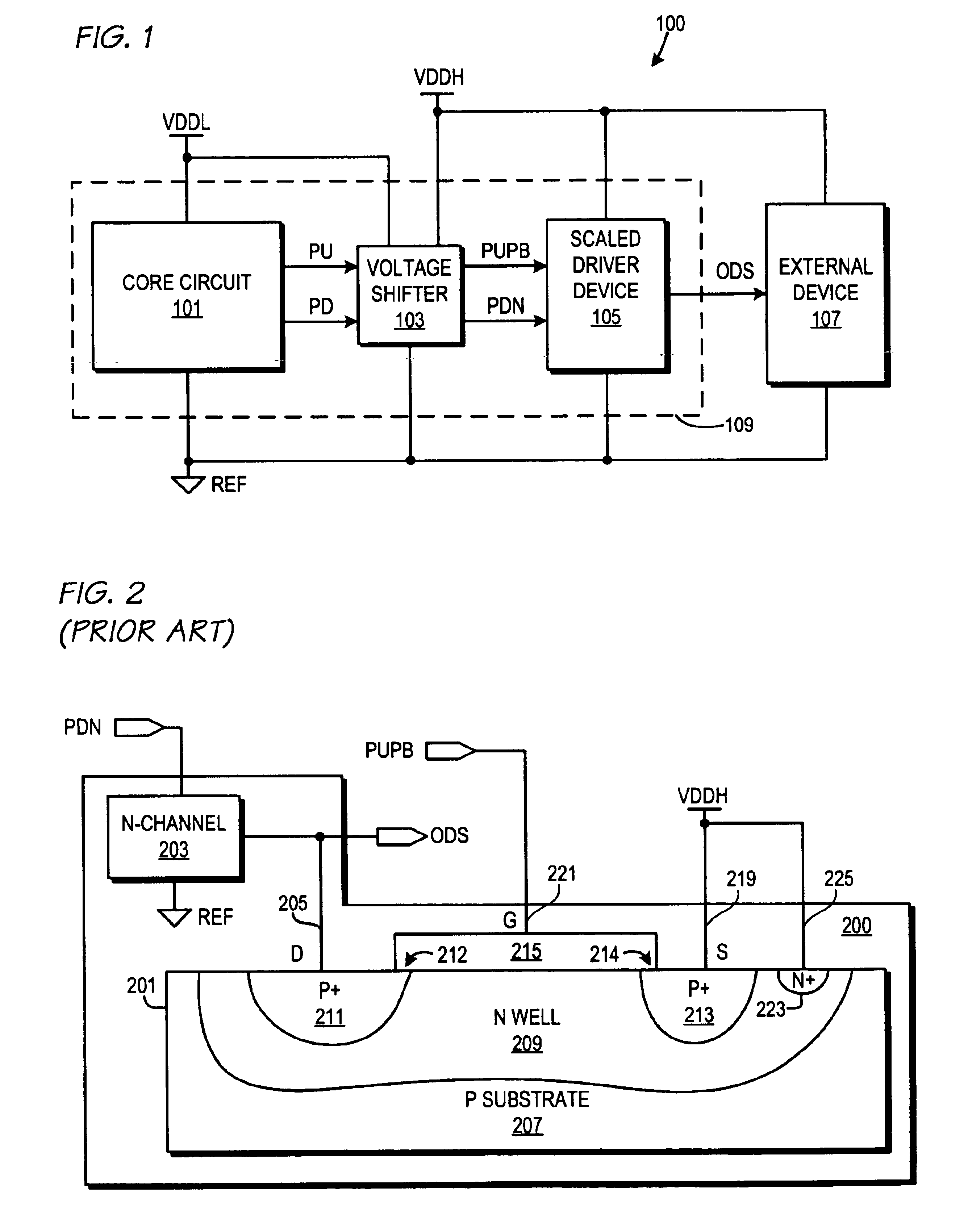
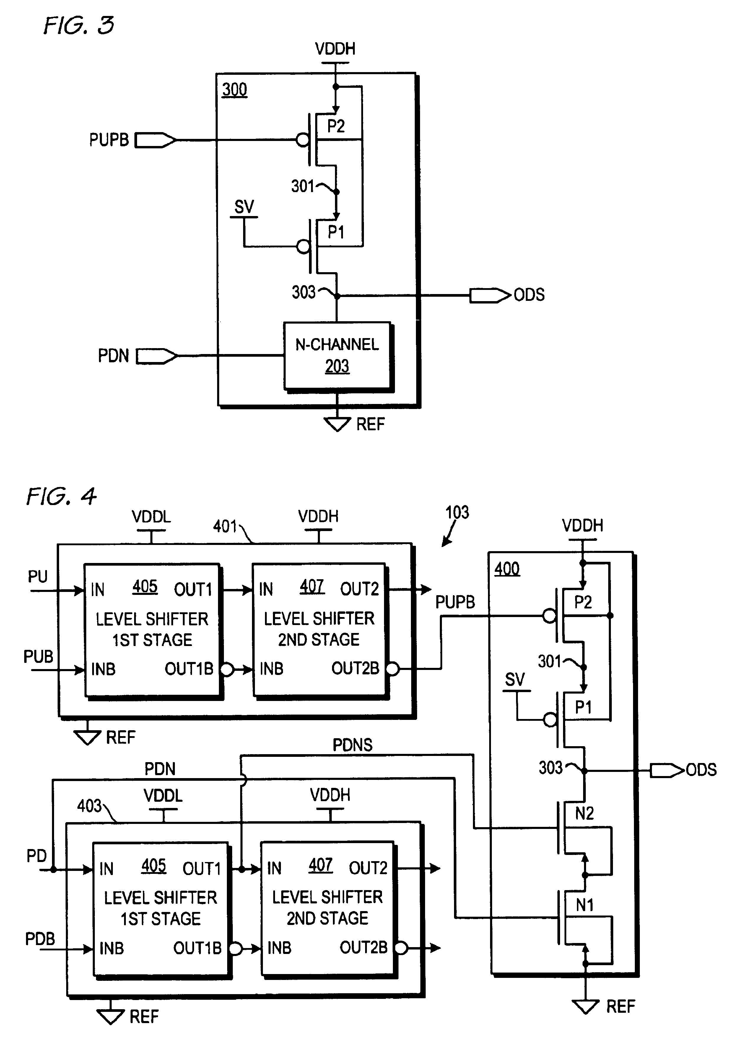
The inventor of the present application has recognized the need for using scaled driver devices that are required to output elevated voltages, such as for driving tri-state buses and the like, but that cannot tolerate elevated voltages levels applied across overlapping gate portions of the device when turned off. The inventor has further recognized the need to avoid hot carrier injec...


PUM


Abstract

An output driver circuit including first and second cascoded scaled P-channel devices coupled to first and second cascoded scaled N-channel devices. The P-channel devices are coupled together at a first node and between an output and a first source voltage having an elevated voltage level. The N-channel devices are coupled between the output and a reference source voltage. The first scaled P-channel device has a gate that receives a pull-up signal and the second scaled P-channel device has a gate coupled to a static voltage. The second P-channel device and the static voltage are configured to protect the first P-channel device from gate oxide breakdown when the first device is turned off. The first N-channel device has a gate receiving a voltage-limited pull-down signal and the second N-channel device has a gate receiving a lower voltage pull-down signal. The cascoded N-channel devices divide load and prevent hot carrier injection effects.

Description

BACKGROUND OF THE INVENTION1. Field of the InventionThis invention relates to scaled driver devices that are provided to interface external devices operating at elevated voltage levels, and more particularly to a thin oxide output driver including scaled P-channel devices that are not subject to oxide breakdown at elevated voltages, and scaled N-channel devices that are not subject to hot carrier injection effects.2. Description of the Related ArtAs integrated circuit design and fabrication techniques have evolved over the years, the trend is that operating voltages have scaled downward along with device size. Very Large Scale Integrated (VLSI) circuits, particularly microprocessors, tend to lead in the area of size and voltage scaling. As a result, VLSI devices which operate at lower voltages are required to interface to external devices, such as input / output (I / O) devices or the like, that have not been scaled to the same extent as the VLSI devices. Nonetheless, the external devic...

Claims


Application Information

Patent Timeline
IPC IPC(8): H03K19/003
CPCH03K19/00315
Inventor LUNDBERG, JAMES R.
Owner IP FIRST
Why Eureka
Try Eureka