
Method and apparatus for monitoring the operation of a wafer handling robot

Inactive Publication Date: 2005-03-22
TAIWAN SEMICON MFG CO LTD
View PDF11 Cites 107 Cited by
  • Summary
  • Abstract
  • Description
  • Claims
  • Application Information

AI Technical Summary

Benefits of technology

Another object of the invention is to provide a monitor as described above which can be easily retrofitted with existing robotic control systems.
Still another object of the invention is to provide a monitor of the type mentioned above which allows real-time monitoring and detection of errors in control signals.

Problems solved by technology

Each of these electrical connecting lines and associated connectors represent opportunities for errors to be introduced into the signals as a result of any of a number of causes, including electrical interference, shorts, open circuits and signal crossover.
Even small errors introduced into the control signals by any of these causes can result in robot malfunctions or transfer errors that in turn can produce wafer breakage or even equipment damage.
The problem of maintaining signal integrity often becomes more difficult as robots age and the related cabling and connectors begin to experience slight deterioration.
In the past, problems with control signal integrity have been detected only after an error has been introduced into the control signals which has produced a corresponding error in the movement of the robot.
Moreover, even after if it is known that there is a problem with signal integrity, it has been very difficult to trace the exact or even general location of the problem.

Method used


Image

  • Method and apparatus for monitoring the operation of a wafer handling robot
  • Method and apparatus for monitoring the operation of a wafer handling robot
  • Method and apparatus for monitoring the operation of a wafer handling robot

Examples


Embodiment Construction

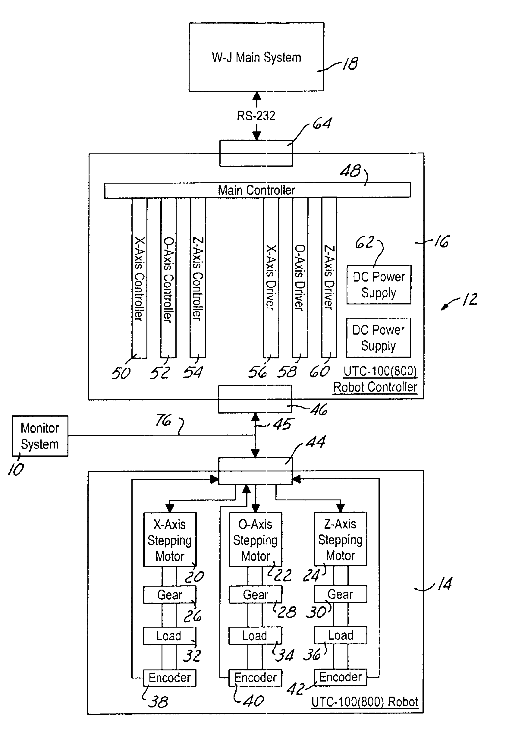
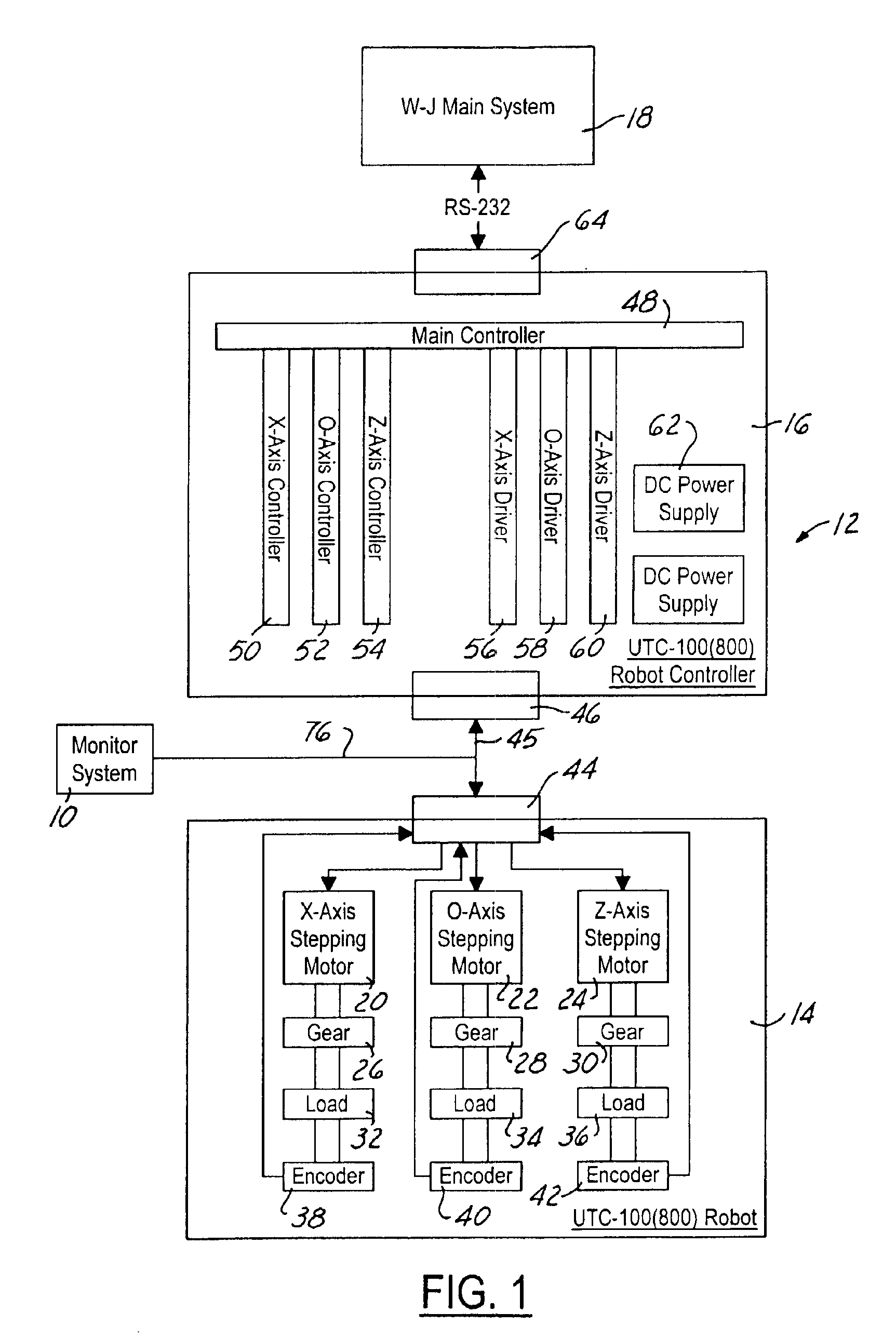
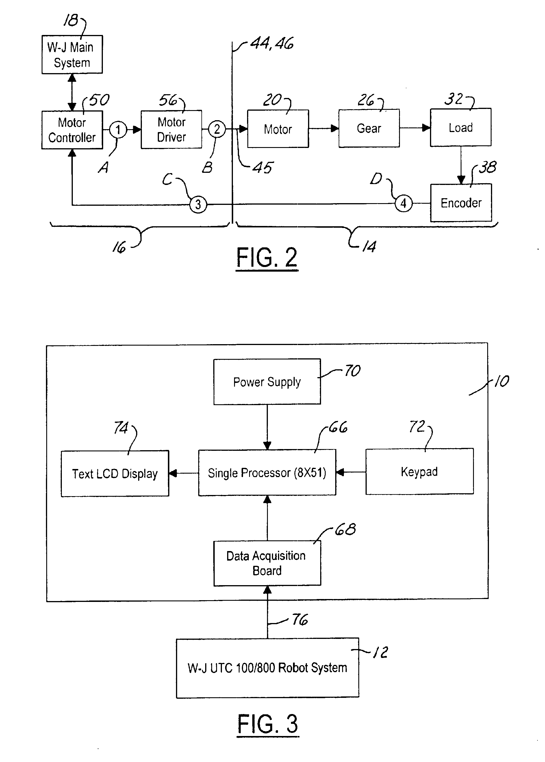
Referring first to FIG. 1, the present invention comprises a monitoring system 10 used to monitor signal integrity in a wafer handling robotic system generally indicated by the numeral 12 which comprises a robot controller 16 and a robotic mechanism 14. The wafer handling robot 12 is communicatively connected via connectors such as the RS-232 connector 64, to a semiconductor processing system 18 which may comprise, for example a single or multiple processing chamber, such as that forming a part of a cluster tool, in which fabrication processes are performed on one or more semiconductor wafers. The wafer handling system 12 functions to transfer one or more wafers within the processing system 18, and between the processing system 18 and a storage location (not shown). A master control system (not shown) operating the processing system 18 sends signals to the handling system 12 through the connector 64 in order to coordinate movements of the handling system 12 with operations in the pr...


PUM


Abstract

The integrity of control signals used to control a wafer handling robot is monitored by a monitor connected to various points of the robotic control system. The monitor includes a memory for storing data sets representing correct, reference characteristics of the control signals. The monitor samples control signals at various points in the control system and compares these sampled signals with the stored reference characteristics in order to determine whether a signal disparity exists. If a disparity exists, the monitor generates an error.

Description

TECHNICAL FIELDThe present invention broadly relates to automated transport systems used in semiconductor manufacturing operations, and deals more particularly with a method and apparatus for monitoring signal integrity in a wafer handling robot system.BACKGROUND OF THE INVENTIONRobotic systems are used extensively in semiconductor device manufacturing operations in order to minimize operator involvement, optimize efficiency and minimize potential contamination during processing. Robots are commonly employed to transfer one or more semiconductor wafers between storage locations and a plurality of processing stations. For example, a single robot is employed in a so-called “cluster tool” which consists of a modular, multi-chamber, integrated processing system. The robot forms part of a central wafer handling module and functions to transfer the wafers between a number of the peripheral process chambers. The robot is controlled by a controller, such as a PLC (programmable logic control...

Claims


Application Information

Patent Timeline
IPC IPC(8): B25J9/16
CPCB25J9/1674G05B2219/42332G05B2219/34454
Inventor HUANG, KUO-LIANGKUO, ENZOCHEN, PATRICKLIN, YUAN-CHICHLAI, CHIH-YILIU, CHUN-HUNG
Owner TAIWAN SEMICON MFG CO LTD
Learn More