Spatially resolved electromagnetic property measurement

Inactive Publication Date: 2005-03-29
THE TRUSTEES OF THE UNIV OF PENNSYLVANIA
View PDF7 Cites 16 Cited by
  • Summary
  • Abstract
  • Description
  • Claims
  • Application Information

AI Technical Summary

Benefits of technology

These features, as well as other features, of the in

Problems solved by technology

A number of works accessing current-voltage (I-V) characteristic of single interfaces also have been reported; however, a major limitation of such techniques is a preset contact pattern, which does not yield spatially resolved information.
Moreover, contact resistance and contact capacitance are included in the measurements, which may decrease accuracy and complicate data interpretation.
Scanning probe microscopy (SPM) techniques have been successfully used to detect stray fields over Schottky double barriers and to image potential drops at lat

Method used


Image

  • Spatially resolved electromagnetic property measurement
  • Spatially resolved electromagnetic property measurement
  • Spatially resolved electromagnetic property measurement

Examples


Embodiment Construction

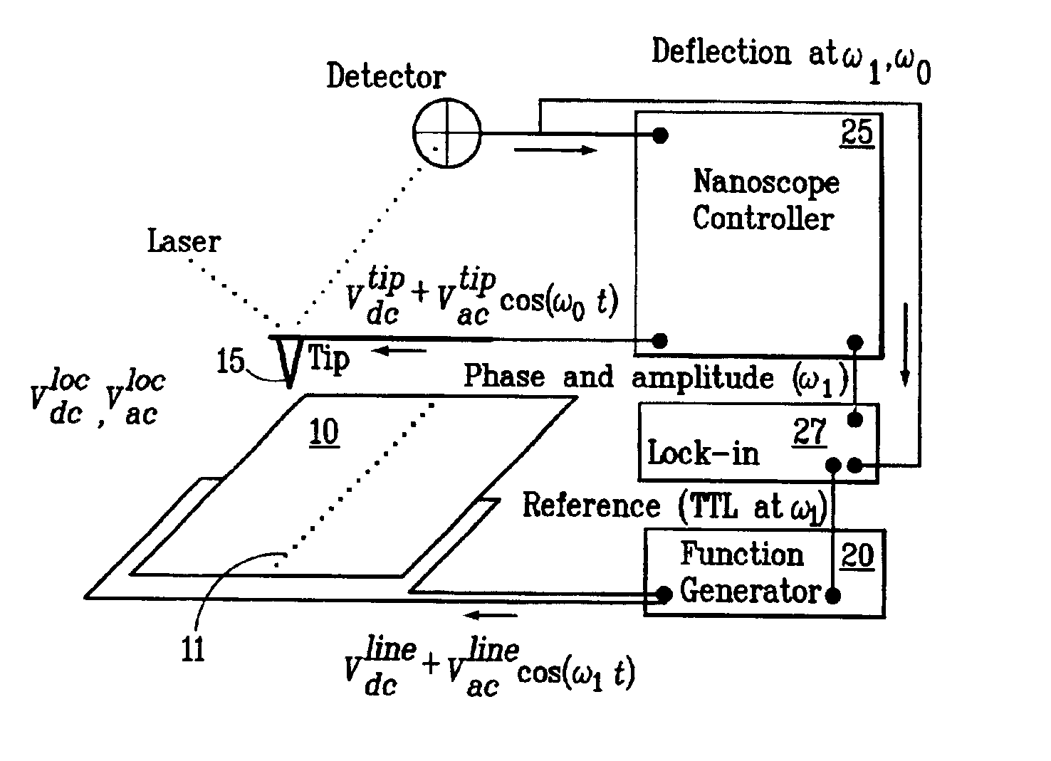
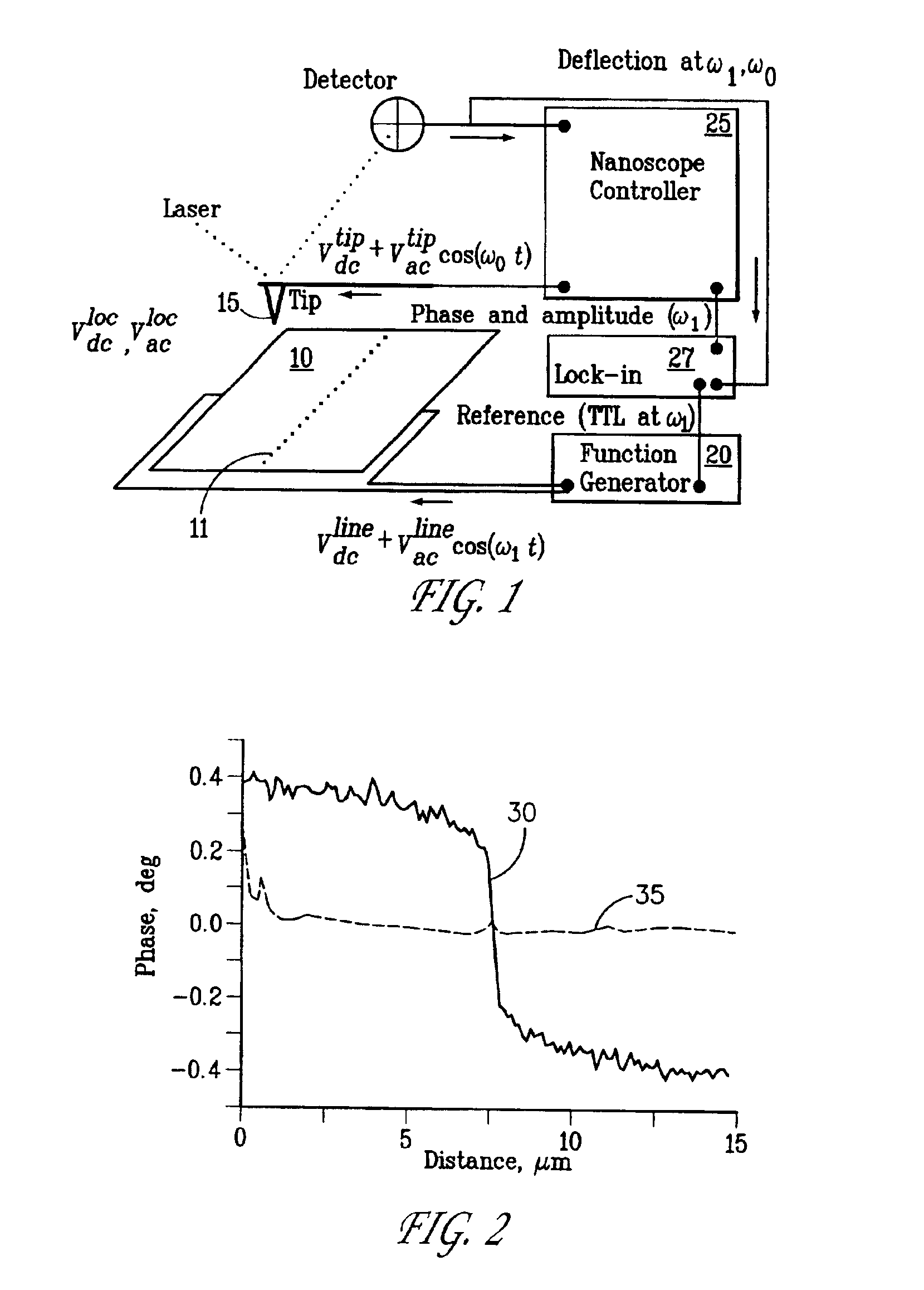
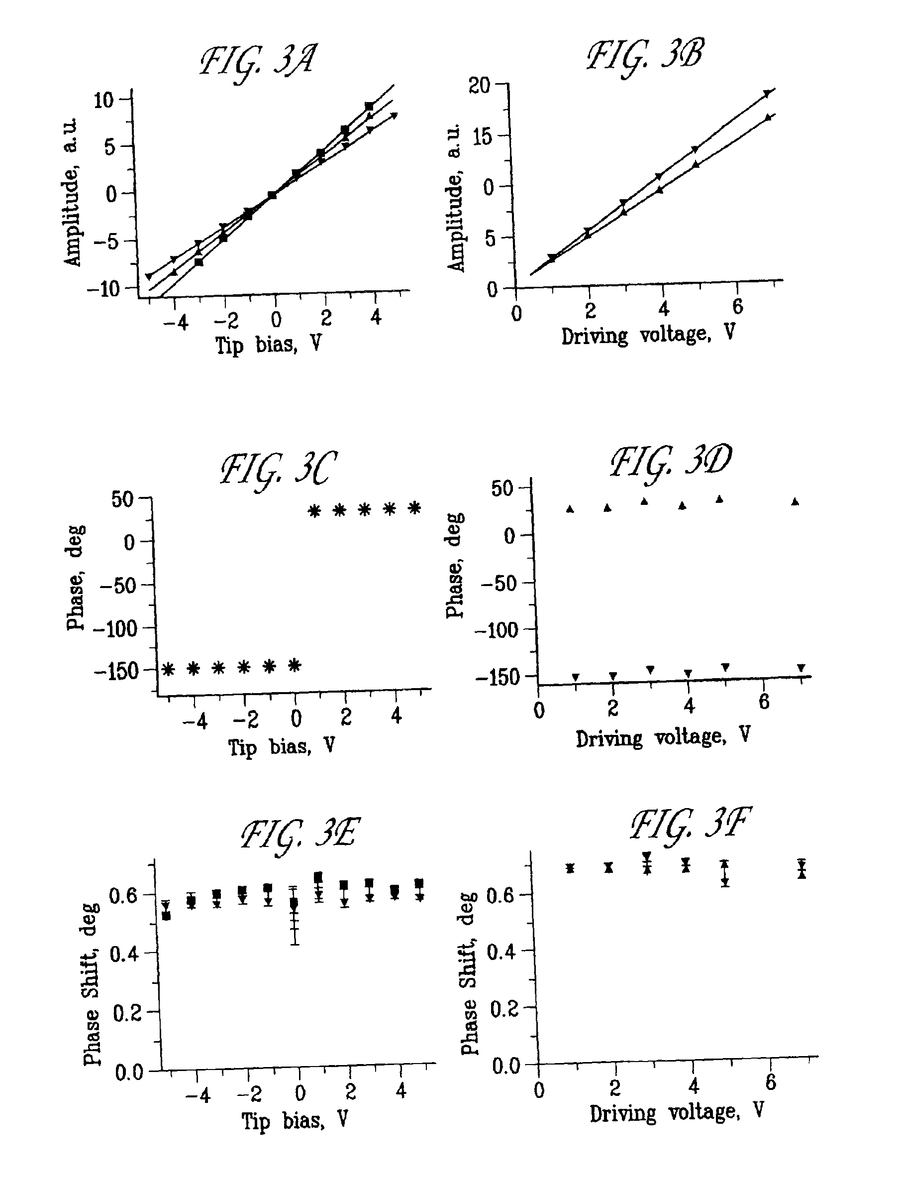
FIG. 1 illustrates a block diagram of a measurement system in accordance with an embodiment of the invention. As shown in FIG. 1, the local impedance of a sample 10 is determined across a grain boundary 11. A bias is laterally applied to the sample 10, across the grain boundary 11, and the deflection of a cantilevered tip 15 is measured. Tip 15 may be magnetic or non-magnetic. For determining grain boundary impedance, tip 15 is typically non-magnetic. The sample bias is applied with a function generator 20. The magnitude and phase of the deflection of cantilevered tip 15 are measured with a conventional atomic-force microscope (AFM) controller 25 (Nanoscope-III, Digital Instruments, Santa Barbara, Calif.). Lock in amplifier 27 is coupled to function generator 20 and AFM controller 25. AFM controller 25 may include a processor for processing measurements taken from tip 15; alternatively a separate processor may be coupled to AFM controller 15.

Tip 15 traverses the tip along a predeter...


PUM


Abstract

A scanning probe detects phase changes of a cantilevered tip proximate to a sample, the oscillations of the cantilevered tip are induced by a lateral bias applied to the sample to quantify the local impedance of the interface normal to the surface of the sample. An ac voltage having a frequency is applied to the sample. The sample is placed at a fixed distance from the cantilevered tip and a phase angle of the cantilevered tip is measured. The position of the cantilevered tip is changed relative to the sample and another phase angle is measured. A phase shift of the deflection of the cantilevered tip is determined based on the phase angles. The impedance of the grain boundary, specifically interface capacitance and resistance, is calculated based on the phase shift and the frequency of the ac voltage. Magnetic properties are measured by applying a dc bias to the tip that cancels electrostatic forces, thereby providing direct measurement of magnetic forces.

Description

FIELD OF THE INVENTIONThe invention relates generally to electromagnetic property measurement, and more particularly, to spatially resolved impedance microscopy of interfaces and to distinguishing surface potential induced forces from magnetically induced forces for current carrying materials.BACKGROUND OF THE INVENTIONMany classes of devices function based on the structure, topology, and other properties of grain boundaries or interfaces. Examples include varistors, PTCR thermistors, diodes, chemical sensors, and solar cells. The properties of interfaces have been extensively studied by macroscopic techniques, such as dc transport measurements and impedance spectroscopy, etc. These techniques address averaged properties of interfaces and little or no information is obtained about the properties of an individual interface. Recently, a number of approaches have been suggested to isolate individual grain boundaries using micropatterned contacts or bicrystal samples. A number of works ...

Claims


Application Information

Patent Timeline
IPC IPC(8): G01R1/067G01R1/07G01R33/038G12B21/02G12B21/00G01Q60/54
CPCB82Y35/00G01R1/071G01R33/0385G01Q60/54B82Y25/00Y10S977/852
Inventor BONNELL, DAWN A.KALININ, SERGEI V.ALVAREZ, RODOLFO ANTONIO
Owner THE TRUSTEES OF THE UNIV OF PENNSYLVANIA
Why Eureka
Try Eureka