

Liquid crystal display panel
a technology of liquid crystal display panel and display panel, which is applied in the direction of non-linear optics, identification means, instruments, etc., can solve the problems of insufficient holding of signal voltage, achieve good quality, prevent display unevenness, and suppress the fluctuation of voltage of storage capacitor bus lines
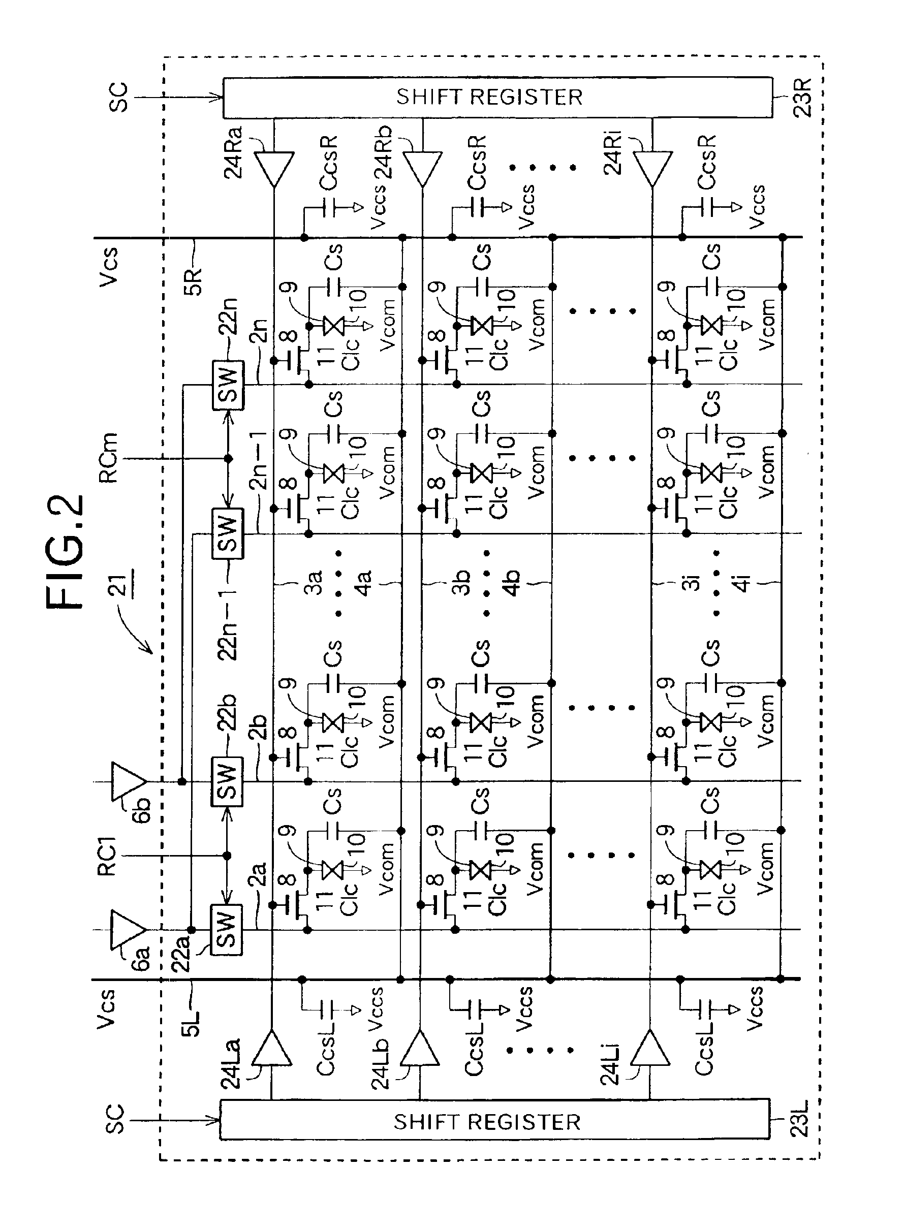
- Summary
- Abstract
- Description
- Claims
- Application Information
AI Technical Summary
Benefits of technology
Problems solved by technology
Method used
Image

Examples
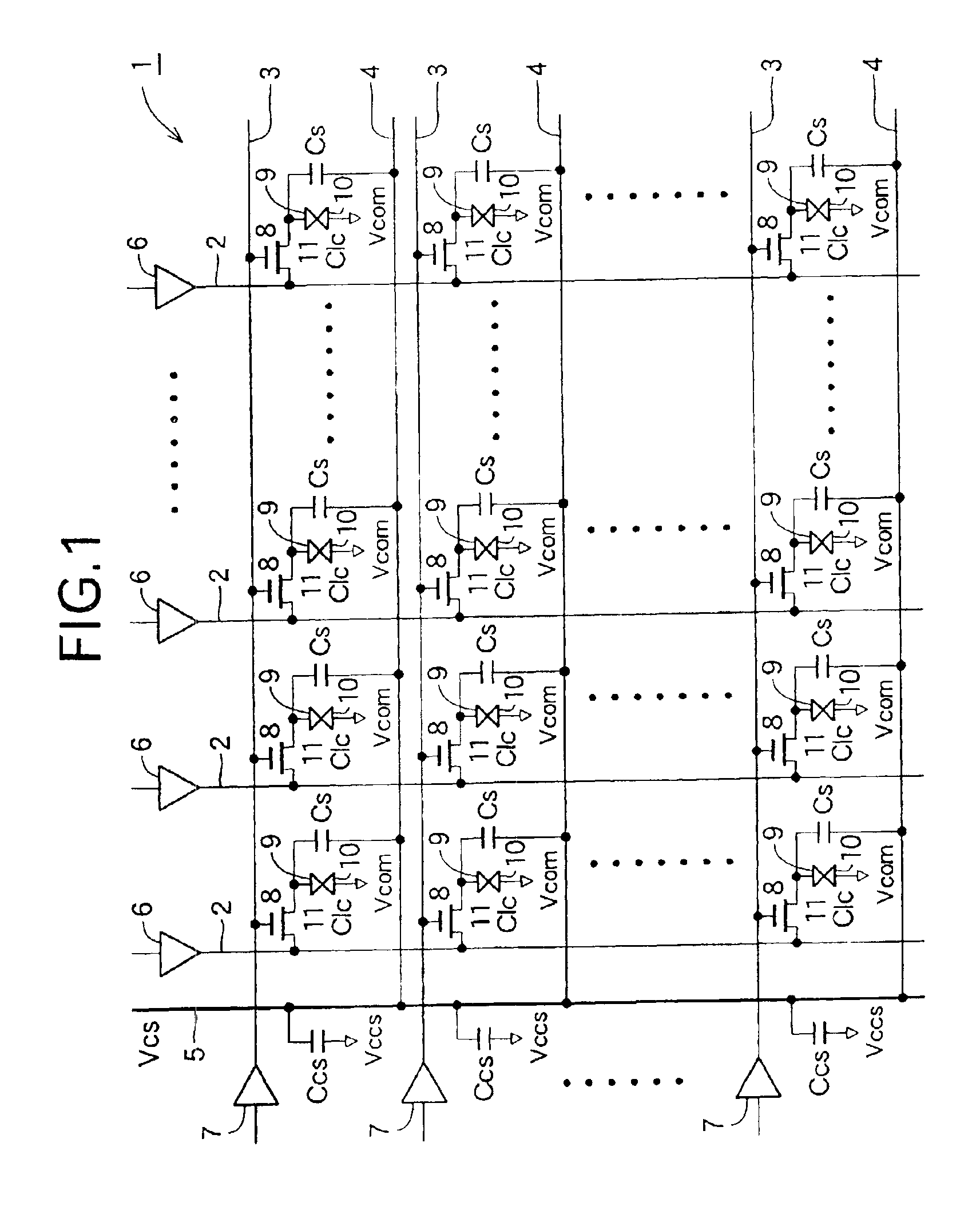
first embodiment
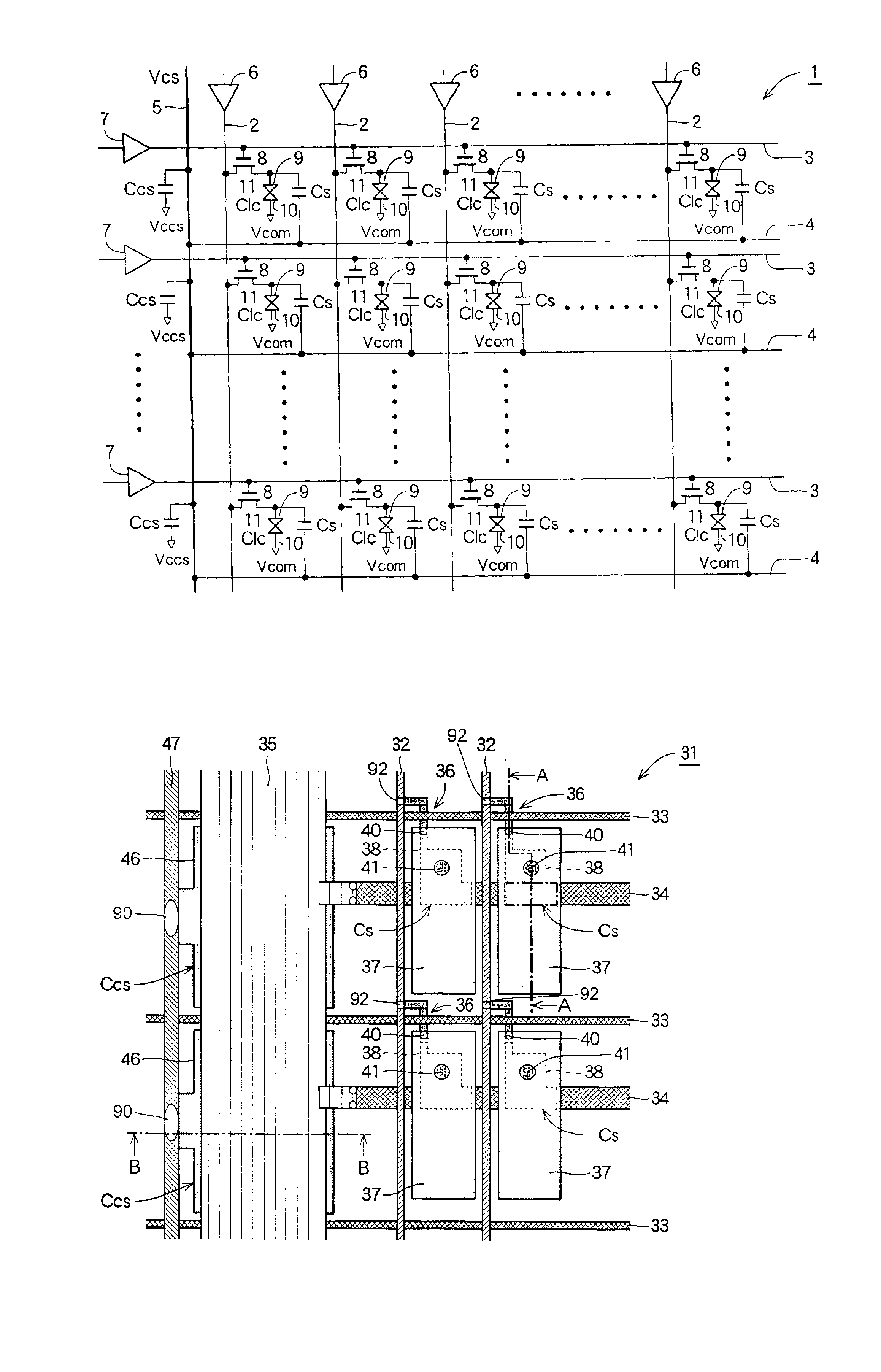
FIG. 3 is a diagram of a wiring constitution of major portions in the liquid crystal display panel FIG. 4A is a sectional view of a pixel region (along the line A—A in FIG. 3), and FIG. 4B is a sectional view of a capacitor portion (along the line B—B in FIG. 3) formed by utilizing the common storage capacitor bus line.
In the liquid crystal display panel 31 according to the first embodiment as shown in FIG. 3, there are formed a plurality of gate bus lines 33 in parallel on the transparent glass substrate, and a plurality of data bus lines 32 intersecting thereto via an insulating film which is not shown. There are further formed a plurality of storage capacitor bus lines (horizontal Cs bus lines) 34 in parallel with the gate bus lines 33, and a common storage capacitor bus line (vertical Cs bus line) 35 in parallel with the data bus lines 32.
TFTs 36 are arranged at positions near the points where the gate bus lines 33 intersect the data bus lines 32. Pixel electrodes (transparent ...
second embodiment
FIG. 5 is a diagram of a wiring constitution of major portions in the liquid crystal display panel according to the invention, FIG. 6A is a sectional view of a pixel region (along the line C—C in FIG. 5), and FIG. 6B is a sectional view of a capacitor portion (along the line D—D in FIG. 5) formed by utilizing the common storage capacitor bus line.
In the liquid crystal display panel 51 according to the second embodiment as shown in FIG. 5, there are formed a plurality of gate bus lines 53 in parallel on the transparent glass substrate, and a plurality of data bus lines 52 intersecting thereto via an insulating film which is not shown. There are further formed a plurality of storage capacitor bus lines (horizontal Cs bus lines) 54 in parallel with the gate bus lines 53, and a common storage capacitor bus line (vertical Cs bus line) 55 in parallel with the data bus line 52.
TFTs 56 are arranged at positions near the points where the gate bus lines 53 intersect the data bus lines 52. The...
third embodiment
FIG. 7 is a diagram of a wiring constitution of major portions in the liquid crystal display panel according to the invention. In the liquid crystal display panel 71 shown in FIG. 7, the storage capacitor Cs of the pixel is formed of an MOS capacitor of n-CH (n-channel), and the auxiliary capacitor Ccs added to the common storage capacitor bus line (vertical Cs bus line) 67 is formed of an MOS capacitor of p-CH (p-channel). The wiring structure of the liquid crystal display panel 71 shown in FIG. 7 is almost the same as the wiring structure of the liquid crystal display panel 51 shown in FIG. 5 except that the polysilicon layer 72 which serves as one electrode of the storage capacitor Cs is formed of polysilicon of n-CH (n-channel) and the polysilicon layer 73 which serves as one electrode of the auxiliary capacitor Ccs added to the common storage capacitor bus line 67 is formed of polysilicon of p-CH (p-channel).
Upon forming the storage capacitor Cs in the n-MOS structure and formi...
PUM
| Property | Measurement | Unit |
|---|---|---|
| voltage | aaaaa | aaaaa |
| voltage | aaaaa | aaaaa |
| transparent | aaaaa | aaaaa |
Abstract
Description
Claims
Application Information