Method for producing a grid structure, an optical element, an evanescence field sensor plate, microtitre plate and an optical communication engineering coupler as well as a device for monitoring a wavelength

a technology of evanescence field sensor and optical communication engineering coupler, which is applied in the direction of fluorescence/phosphorescence, instruments, photomechanical equipment, etc., can solve the problems of hardly being able to avoid stitching errors during electron beam writing, requiring very long processing times, and requiring more than 1 mm gratings. , to achieve the effect of high precision, low effort and high precision

Inactive Publication Date: 2005-03-29
OERLIKON TRADING AG TRUEBBACH
View PDF6 Cites 52 Cited by
  • Summary
  • Abstract
  • Description
  • Claims
  • Application Information

AI Technical Summary

Benefits of technology

It is the object of the invention to provide a process which permits the production, particularly the volume production, of lattice structures with high precision and relatively low effort.
Using the process according to the invention it is also possible to produce large-area lattice structures, particularly continuous grating structures which are long in a direction parallel to the lines, with high precision throughout, and in a simple and economical way. Moreover, a large freedom of design is secured with respect to the arrangement and shape of the grating structures. Hence the production of highly different optical elements for diverse applications is feasible with one and the same installations. The process according to the invention furthermore permits the production of large series of optical elements of constant quality and with optical properties such as coupling efficiencies and, in particular, coupling angles which are constant within narrow limits.
Furthermore, a highly precise optical element is to be provided such as can be produced by the process according to the invention. In particular, the optical element can be formed as an evanescent field sensor plate or as a microtitre plate based on such a plate. In view of the narrow limits within which, even in long gratings, the coupling angle varies, it is possible to simultaneously illuminate and read out larger parts of the evanescent field sensor plate or microtitre plate. Successive exposure of different parts of the evanescent field sensor plate or microtitre plate is also simplified since reoptimisation of the relative angular position of this plate and the exposing unit is not required or in any case greatly simplified.
The optical element can also be formed as an optical coupler for communications technology. In this case, the high precision present even in large grating structures guarantees excellent filter characteristics, and particularly a very-narrow-band selection of individual wavelengths, so that for instance a wavelength multiplexing involving very closely spaced wavelengths is possible, which raises the transmission capacity.

Problems solved by technology

Greater lengths are possible but require very long processing times. In practice, gratings of more than 1 mm2 can scarcely be produced with reasonable effort and good accuracy.
In particular, stitching errors can hardly be avoided during electron beam writing.
All plates described above are produced by processes with which no satisfactory uniformity of the coupling grating can be achieved, so that the coupling angle varies relatively widely.
The filter characteristics are unsatisfactory and not sufficient, for instance, for selectively filtering a particular wavelength from a group of very closely spaced wavelengths, when the plate is used as an optical coupler in communications technology.
Some of the processes described are also very laborious or do not allow very large numbers of pieces of constant quality to be made.

Method used


Image

  • Method for producing a grid structure, an optical element, an evanescence field sensor plate, microtitre plate and an optical communication engineering coupler as well as a device for monitoring a wavelength
  • Method for producing a grid structure, an optical element, an evanescence field sensor plate, microtitre plate and an optical communication engineering coupler as well as a device for monitoring a wavelength
  • Method for producing a grid structure, an optical element, an evanescence field sensor plate, microtitre plate and an optical communication engineering coupler as well as a device for monitoring a wavelength

Examples


Embodiment Construction

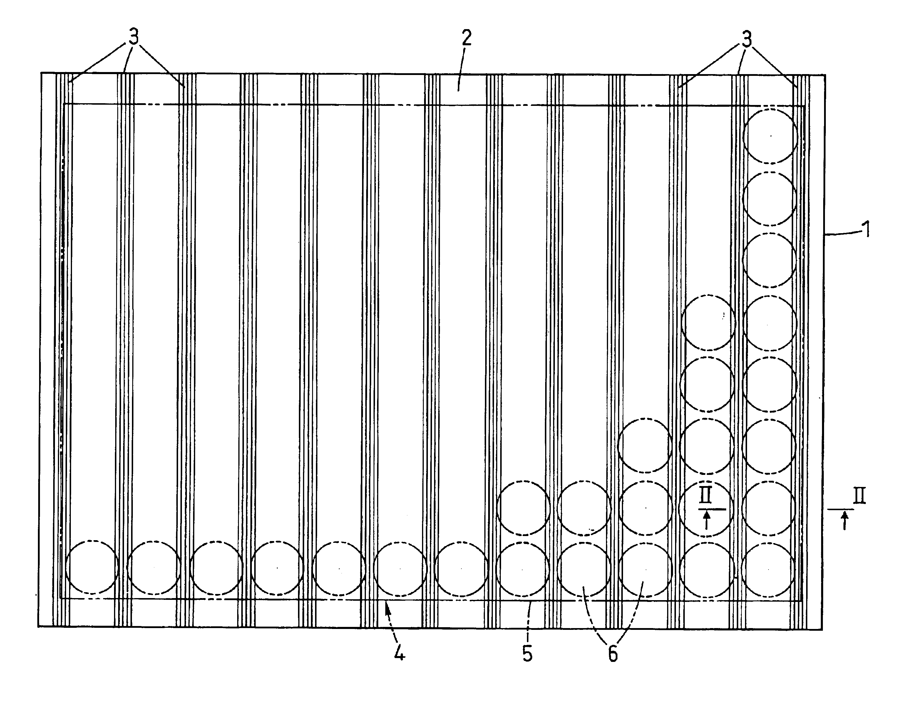
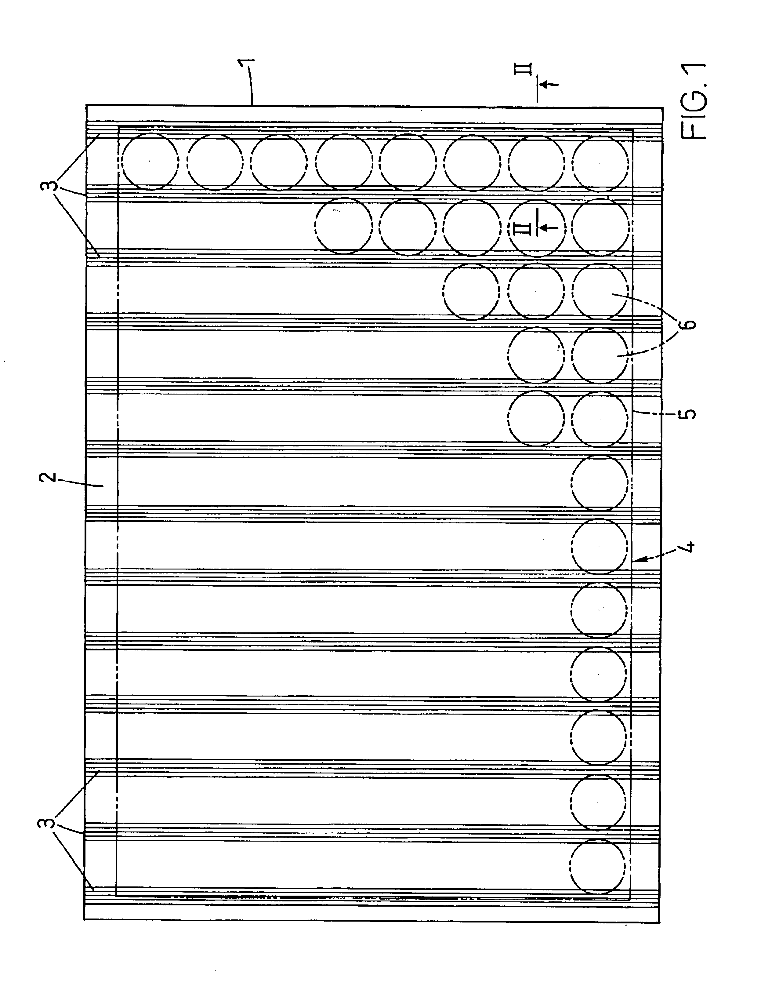
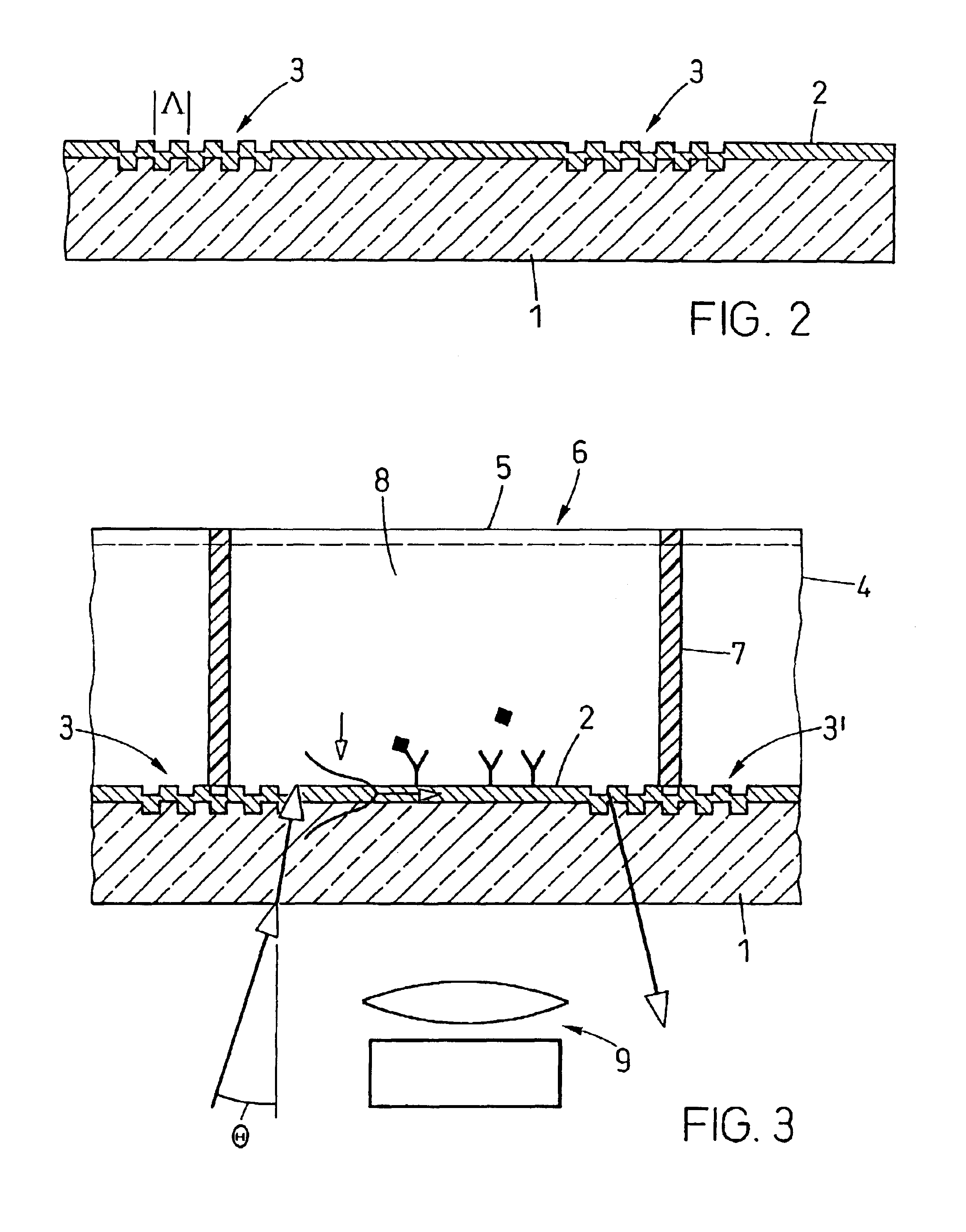
The process according to the invention will in the following be explained in more detail in connection with an evanescent field sensor plate and its production. Here, an evanescent field sensor plate is understood as a plate making it possible by illumination of one part of the surface to create an evanescent field in the reach of which a sample to be analysed may be arranged. Therefore, evanescent field sensor plates serve the purposes of chemical analysis. Evanescent fields are nonradiating electromagnetic fields which fall off and vanish with increasing distance from the scattering surface at which they are generated. Such fields can arise in connection with spatial modulations of the electric field in the plane having periodicities smaller than one wavelength. The best-known example of such a modulation occurs at an interface between a dielectric and air when a light beam coming from the side of the dielectric has an angle of incidence larger than the critical angle.

Evanescent f...


PUM

PropertyMeasurementUnit
surface areaaaaaaaaaaa
coupling angleaaaaaaaaaa

Abstract

A coupling grating formed as a line grating with a grating period between 100 nm and 2500 nm, a substrate (1) is covered with a photoresist layer (10) and exposed for instance at the Lithrow angle (ΘL) or at 0° to a mercury-vapour lamp (11) via a folding mirror (13, 13′) through a phase mask (14) in the near field of which the photoresist layer is arranged, then structured by reactive ion etching and provided with a transparent layer by reactive DC magnetron sputtering, particularly pulsed DC sputtering or AC-superimposed DC sputtering. The phase mask (14) is structured in advance with the laser two-beam interference method. The process is particularly suited for the production of optical elements, particularly evane-scent field sensor plates and optical couplers for communications technology which can be employed in particular as filters for wavelength multiplexing in fibre-optic networks.

Description

FIELD OF THE INVENTIONThe invention relates to a process for producing at least one continuous grating structure an optical element produced with the aid of the process according to the invention, as well as an evanescent field sensor plate and a microtitre plate and an optical coupler for communications technology, furthermore a device for monitoring a wavelength containing such a coupler.The process according to the invention is suitable for producing optical elements with grating structures. Evanescent field sensor plates and microtitre plates produced according to the process can be used in chemical and biomolecular analyses. The applications of optical couplers are in communications technology, and more particularly in data transmission via fibre networks. A potential application of a particular coupler according to the invention is in a device for monitoring the wavelength of laser light in a fibre network.PRIOR ARTFrom EP-A-0 602 829 a process for producing a grating structur...

Claims


Application Information

Patent Timeline
Patent Type & Authority Patents(United States)
IPC IPC(8): G01N21/55G02B6/124G02B6/34G02B6/12G01N21/552G01N21/64G01N21/77G01N33/53G01N37/00G02B5/18G02B6/02G02B6/122G02B6/13
CPCG01N21/552G01N21/7703G01N21/7743G02B6/12007G02B6/124G02B6/34G01N2021/7776G02B2006/12107G02B6/02138G01N21/648
Inventor MAISENHOLDER, BERNDEDLINGER, JOHANNESHEINE, CLAUSPAWLAK, MICHAELDUVENECK, GERT
Owner OERLIKON TRADING AG TRUEBBACH
Why Eureka
Try Eureka