Lead frame, method of manufacturing the same, and method of manufacturing a semiconductor device using the same

a technology of lead frame and manufacturing method, which is applied in the direction of semiconductor devices, semiconductor/solid-state device details, electrical apparatus, etc., can solve the problems of frame warping, lowering reliability as semiconductor devices, and difficulty in efficient package assembly compared to mass molding methods, so as to reduce the warping step without increasing the load on the taping step , the effect of reducing the frame warping

Inactive Publication Date: 2005-04-05
SHINKO ELECTRIC IND CO LTD
View PDF7 Cites 5 Cited by
  • Summary
  • Abstract
  • Description
  • Claims
  • Application Information

AI Technical Summary

Benefits of technology

An object of the present invention is to provide a lead frame capable of effectuating partial taping without increasing the load on the taping step and thereby capabl

Problems solved by technology

However, since a resin molding is individually performed for each of the semiconductor elements in the individual molding method, there is a difficulty in terms of an efficient package assembly as compared to the mass molding method.
However, since the adhesive tape is attached to one of the surfaces of the lead frame as mentioned above, a problem occurs in the event of a heat treatment in the molding step in that the lead frame is

Method used


Image

  • Lead frame, method of manufacturing the same, and method of manufacturing a semiconductor device using the same
  • Lead frame, method of manufacturing the same, and method of manufacturing a semiconductor device using the same
  • Lead frame, method of manufacturing the same, and method of manufacturing a semiconductor device using the same

Examples


first embodiment

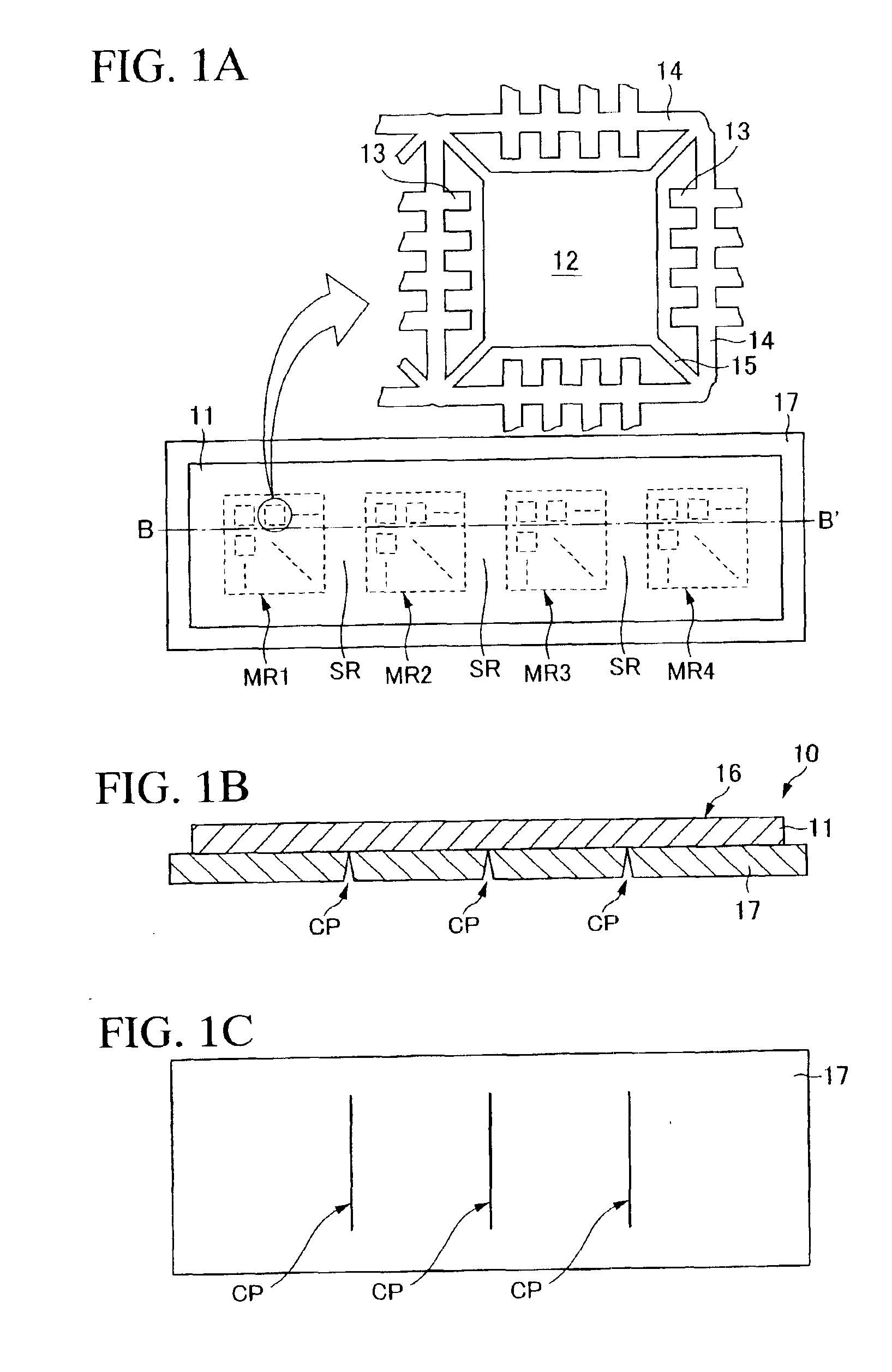
FIG. 1A to FIG. 1C schematically show a constitution of a lead frame according to the present invention. In the drawings, FIG. 1A shows a plan-view constitution of the lead frame viewed from one surface thereof (the side on which regions for resin-molding semiconductor elements to be mounted are defined), FIG. 1B shows a cross-sectional structure of the lead frame viewed along B-B′ line in FIG. 1A, and FIG. 1C shows a plan-view structure of the lead frame viewed from the other surface thereof (the opposite side to the side on which the resin-molding regions are defined), respectively.

A lead frame 10 according to this embodiment is basically composed of a base frame 11 to be used as a substrate of a QFN. As shown in FIG. 1A, a plurality of resin-molding regions MRi (i=1 to 4) are defined separately in land shapes on one surface of the base frame 11. A plurality of semiconductor elements are mounted on each of the resin-molding regions MRi as described later, which are resin-molded by...

third embodiment

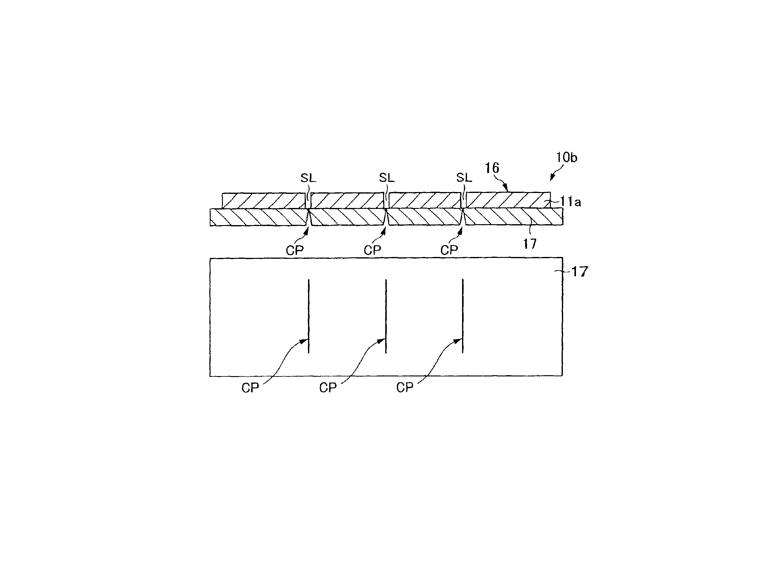
FIG. 4A to FIG. 4C schematically show a constitution of a lead frame according to the present invention.

A lead frame 10b according to the third embodiment is different from the lead frame 10 shown in FIG. 1A to FIG. 1C in that slits SL are formed at portions of a base frame 11a corresponding to the portions of the adhesive tape 17 on which cut portions CP are provided. Other constitution is the same as the first embodiment (FIG. 1A to FIG. 1C), and thus description thereof will be omitted.

Hereinafter, description will be made with respect to a method of manufacturing the lead frame 10b of this embodiment with reference to FIG. 5A to FIG. 5D collectively showing the manufacturing steps thereof.

In the first step (FIG. 5A), a metal plate (a Cu plate or a Cu-based alloy plate, for example) is patterned by either etching or stamping to form the base frame 11a.

As schematically shown in an upper part of FIG. 5A, the base frame 11a to be formed has a structure in which a plurality of resin...


PUM


Abstract

In a method of manufacturing a lead frame for use in a leadless package such as a quad flat non-leaded package (QFN), a base frame is first formed which includes a region for resin-molding a plurality of semiconductor elements to be mounted on one surface of the base frame, the region being partitioned into land shapes, and in which a die-pad portion and lead portions around the die-pad portion are defined severally for the individual semiconductor elements to be mounted in each of the partitioned regions for resin-molding. Next, an adhesive tape is attached to the other surface of the base frame, and subsequently a cut portion is provided at a portion corresponding to a region between two adjacent partitioned regions for resin-molding, of the adhesive tape.

Description

BACKGROUND OF THE INVENTION(a) Field of the InventionThe present invention relates to a lead frame used as a substrate of packages for mounting semiconductor elements. More specifically, it relates to a lead frame for use in a leadless package such as a quad flat nonleaded package (QFN), a small outline non-leaded package (SON), or the like, which is molded with resin by a mass molding in an assembly process of the packages, also to a method of manufacturing the lead frame and to a method of manufacturing a semiconductor device using the lead frame.(b) Description of the Related ArtWhen a leadless package such as a QFN is fabricated, a basic process thereof includes the steps of mounting semiconductor elements severally on die-pad portions of a lead frame (die bonding), electrically connecting electrodes of the semiconductor elements to lead portions of the lead frame with bonding wires (wire bonding), molding the semiconductor elements, the bonding wires and the like with molding r...

Claims


Application Information

Patent Timeline
IPC IPC(8): H01L23/495H01L21/02H01L23/48H01L21/48H01L21/56H01L21/60H01L21/68H01L23/50
CPCH01L21/4839H01L21/568H01L23/49572H01L24/97H01L21/561H01L2924/01006H01L2224/48091H01L2224/48247H01L2224/85001H01L2224/97H01L2924/01004H01L2924/01027H01L2924/01029H01L2924/01033H01L2924/01038H01L2924/01046H01L2924/01078H01L2924/01079H01L2924/01082H01L2924/18165H01L2924/01005H01L24/48H01L2924/00014H01L2224/85H01L2224/05599H01L2224/45099H01L2224/85399H01L2924/181H01L2924/00012H01L2224/45015H01L2924/207H01L21/60
Inventor KASAHARA, TETSUICHIROTANAKA, HIDETO
Owner SHINKO ELECTRIC IND CO LTD
Why Eureka
Try Eureka