Method for forming quadruple density sidewall image transfer (SIT) structures

a technology of image transfer and sidewall, applied in the direction of basic electric elements, electrical equipment, semiconductor devices, etc., can solve the problems of increasing the cost of advanced photo tooling, increasing the cost of consumables, and increasing the cost of resist, so as to achieve the effect of better balance line space siz

Inactive Publication Date: 2005-04-05
IBM CORP
View PDF2 Cites 285 Cited by
  • Summary
  • Abstract
  • Description
  • Claims
  • Application Information

AI Technical Summary

Benefits of technology

A principal object of the present invention is to provide a method for forming a quadruple density sidewall image transfer (SIT) structure. Other important objects of the present invention are to provide such method for forming a quadruple density sidewall image transfer (SIT) structure substantially without negative effect and that overcome many of the disadvantages of prior art arrangements.
In accordance with features of the invention, the method of the invention enables formation of four well-controlled lines for each lithographically minimum pitch dimension. The method of the invention employs spacers-on-spacers, with one spacer formed utilizing oxidation to better balance line space sizes.

Problems solved by technology

Photolithography is, however, finding progress increasingly expensive and difficult.
Cost of advanced photo tooling continues to significantly increase and costs of consumables, such as resist, are also skyrocketing.
These techniques introduce errors and, of course, additional expense.

Method used


Image

  • Method for forming quadruple density sidewall image transfer (SIT) structures
  • Method for forming quadruple density sidewall image transfer (SIT) structures
  • Method for forming quadruple density sidewall image transfer (SIT) structures

Examples


Embodiment Construction

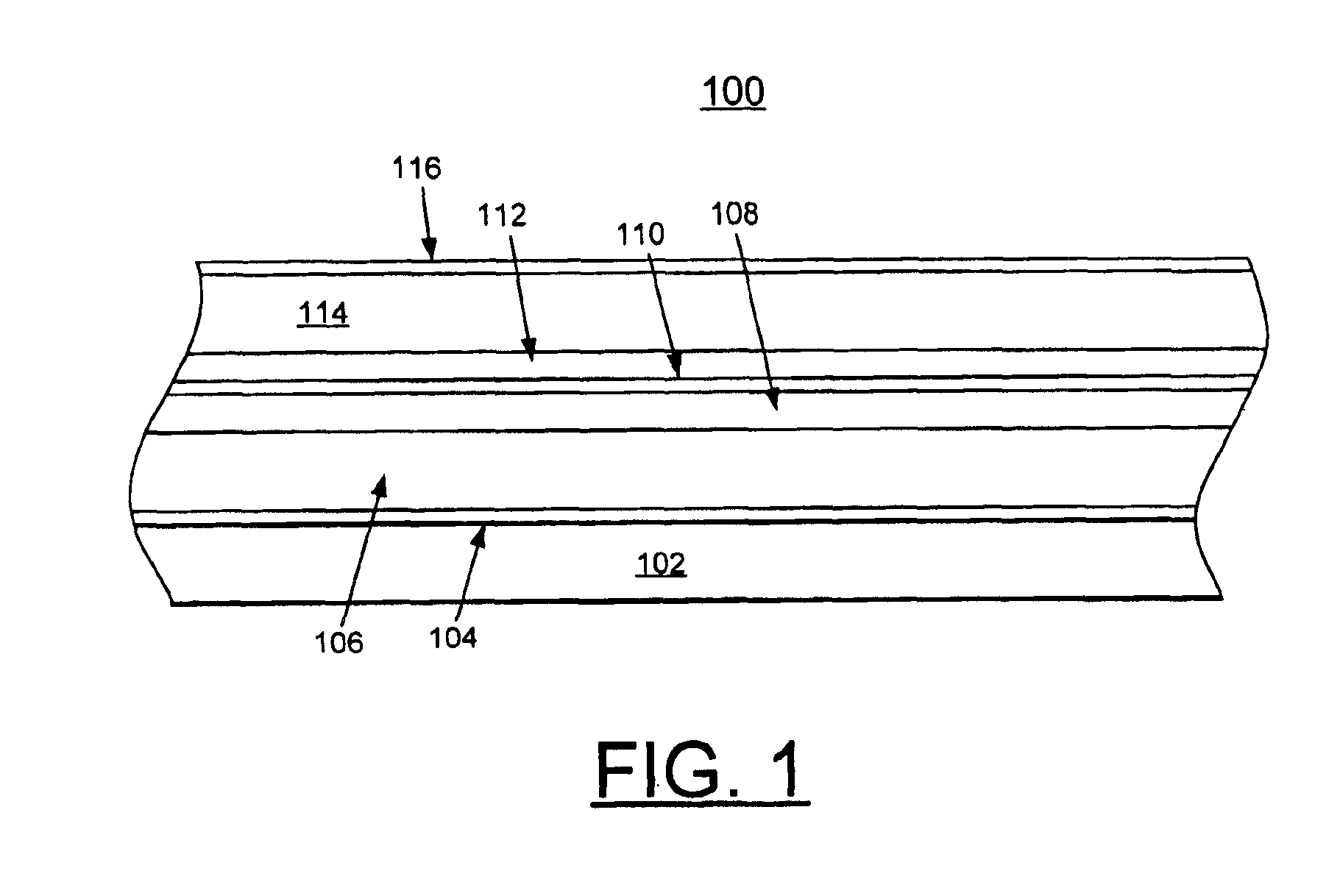
Sidewall Image Transfer (SIT) techniques form conductors with very narrow widths or semiconductor devices with very short gate lengths without using critical photolithography. Sidewall Image Transfer has been proposed as a way to produce well-controlled images having sub-lithographic dimensions.

Use of sidewall spacers to define feature dimensions offers an opportunity to build two shapes using each starting shape since each starting shape, for example, printed using standard lithography, has two edges. Resulting features thus can have half the pitch possible using the same lithographic tools in a conventional printing process. It is desirable to extend the frequency doubling opportunity to even smaller dimensions.

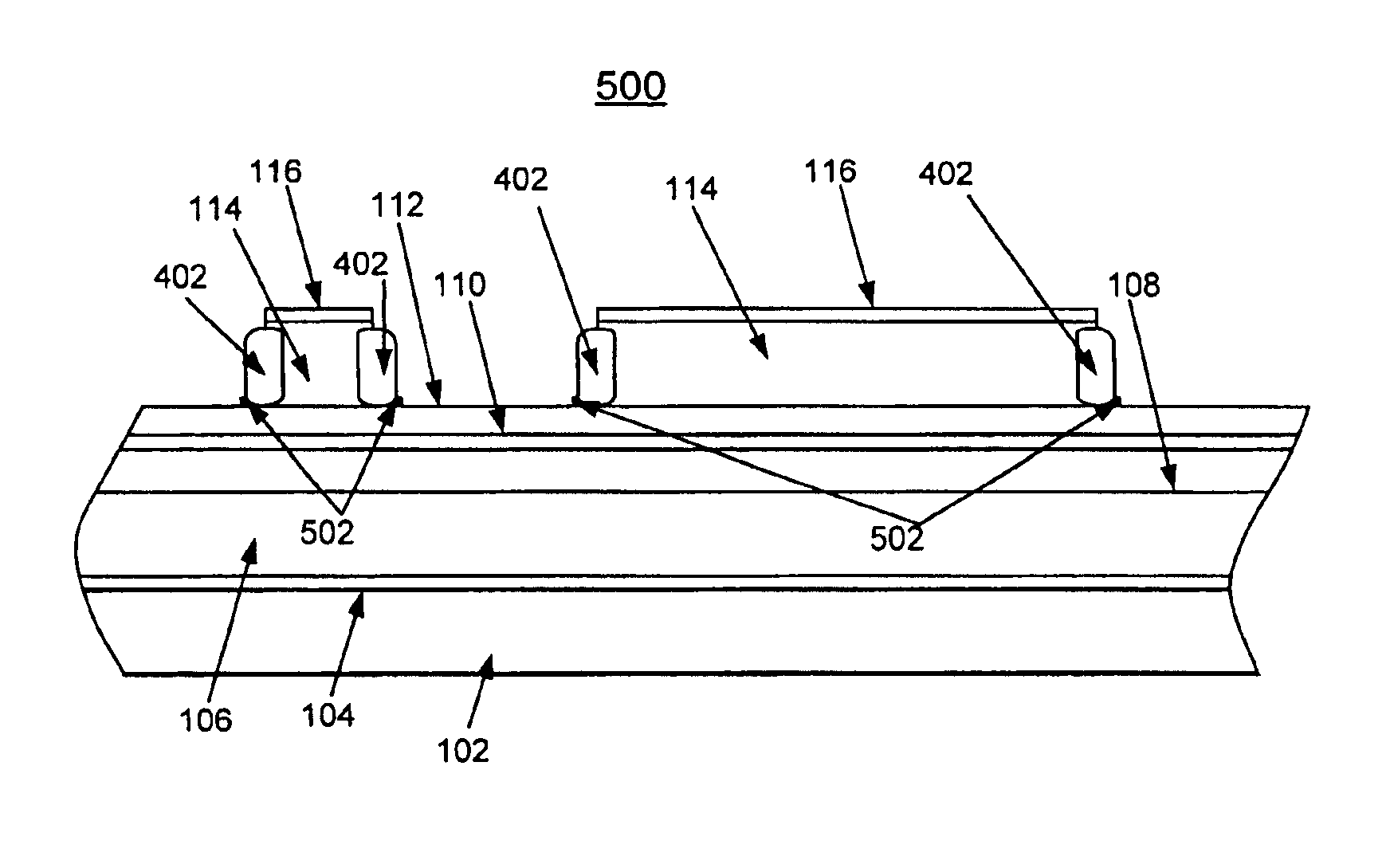
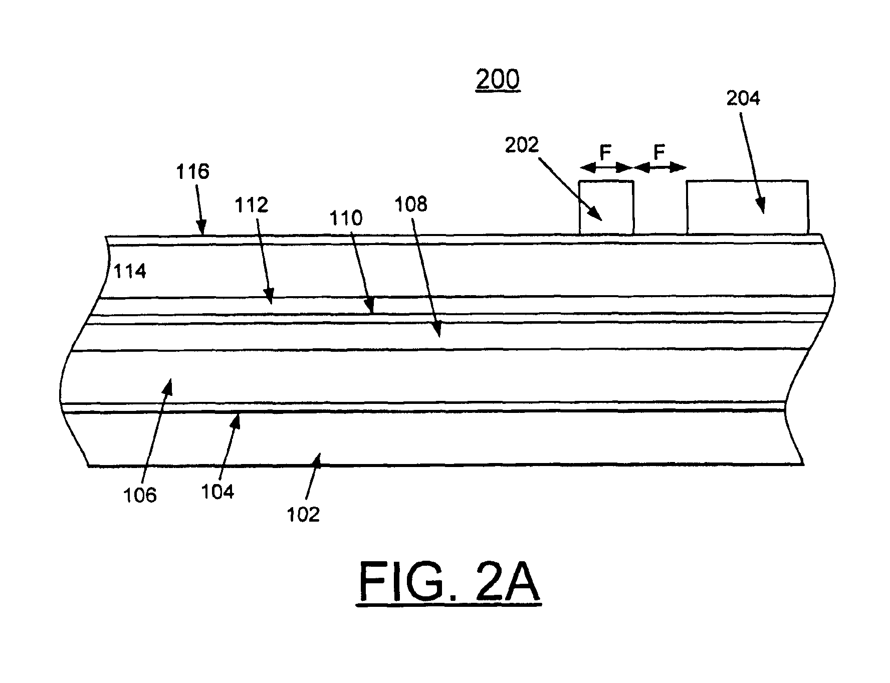
In accordance with features of the preferred embodiment, an extension of the sidewall image transfer (SIT) approach is provided to enable formation of four well-controlled lines for each lithographically minimum pitch dimension. The method of the preferred embodiment is to ...


PUM


Abstract

A method is provided for forming a quadruple density sidewall image transfer (SIT) structure. Oxide spacers are formed on opposite sidewalls of a first mandrel. The oxide spacers form a second mandrel. Then sidewall spacers are formed on opposite sidewalls of the oxide spacers forming the second mandrel. A pattern of the sidewall spacers is used to form the quadruple density sidewall image transfer (SIT) structure. The method of the invention enables formation of four well-controlled lines for each lithographically minimum pitch dimension.

Description

FIELD OF THE INVENTIONThe present invention relates generally to the field of semiconductor manufacturing and, more specifically, to a method for forming a quadruple density sidewall image transfer (SIT) structure.DESCRIPTION OF THE RELATED ARTImprovements in photolithography are driving continued shrinkage of dimensions in advanced semiconductor manufacturing. Photolithography is, however, finding progress increasingly expensive and difficult. Cost of advanced photo tooling continues to significantly increase and costs of consumables, such as resist, are also skyrocketing.Meeting line width objectives has also required introduction of many new ways of enhancing traditional processes such as mask making and data preparation. These techniques introduce errors and, of course, additional expense.It is highly desirable to provide a method which can meet or exceed line width control objectives for future technologies without requiring the use of new and more expensive tooling.SUMMARY OF ...

Claims


Application Information

Patent Timeline
Patent Type & Authority Patents(United States)
IPC IPC(8): H01L21/02H01L21/461H01L21/033H01L21/28H01L21/3213
CPCH01L21/0337H01L21/32139H01L21/28132H01L21/0338
Inventor FURUKAWA, TOSHIHARUHAKEY, MARK CHARLESHOLMES, STEVEN JOHNHORAK, DAVID VACLAVKOBURGER, III, CHARLES WILLIAMMITCHELL, PETER H.
Owner IBM CORP
Why Eureka
Try Eureka