Method for analyzing defect data and inspection apparatus and review system

Inactive Publication Date: 2005-04-05
HITACHI HIGH-TECH CORP +1
View PDF6 Cites 58 Cited by
  • Summary
  • Abstract
  • Description
  • Claims
  • Application Information

AI Technical Summary

Benefits of technology

According to the invention, since a high-density region image representing a high-density portion of defects is generated on the basis of the position coordinates of defects detected by an inspection apparatus, the high-density region is not required to recognize as cluster, and a relatively high-density region can be extracted even if the distribution is thin. Moreover, according to the inventio

Problems solved by technology

Therefore, it cannot be used for the distribution that is so thin that the cluster cannot be recognized.
For auto

Method used


Image

  • Method for analyzing defect data and inspection apparatus and review system
  • Method for analyzing defect data and inspection apparatus and review system
  • Method for analyzing defect data and inspection apparatus and review system

Examples


first embodiment

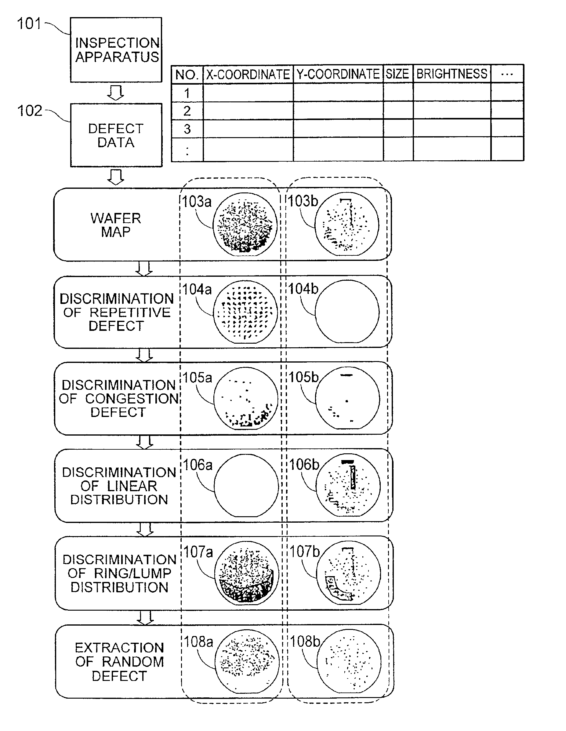
the inspection apparatus having the defect data analysis method according to the invention will be described. Hereafter, repetitive defect, congestion defect, linear distribution defect, ring / lump distribution defect and random defect are called distribution feature category. Known inspection apparatus for semiconductor substrate include foreign substance inspection apparatus, optical type pattern defect inspection apparatus and SEM type pattern defect inspection apparatus. The inspection apparatus according to the invention makes inspection for semiconductor substrate by the same known method as either one of these inspection apparatus, classifies the obtained defect data into the distribution feature category by the above method and produces the category information together with the defect data information.

FIG. 15 is a diagram of the construction of the first embodiment of the inspection apparatus according to the invention.

Pattern information adding means 301 adds pattern-relate...

second embodiment

FIG. 16 shows the construction of the inspection apparatus according to the invention.

The pattern information adding means 301 adds sampling condition number in addition to the above information. It manually groups the dictionary patterns using the same sampling condition, and attaches the same sampling number. When there is no sampling condition corresponding to the number, sampling condition generation means 307 generates the sampling condition.

The sampling condition generation means 307 generates the sampling condition for determining a defect for review. It manually generates the sampling conditions associated with the patterns of ring / lump distribution defects, and sampling conditions at each of the other distribution feature categories, and makes them be stored as a sampling condition file 312 in the storage means 302. The sampling conditions are, for example, sampling number, sampling rate and sampling method. The values of sampling number and sampling rate are entered after ...


PUM


Abstract

The distribution states of defects are analyzed on the basis of the coordinates of defects detected by an inspection apparatus to classify them into a distribution feature category, or any one of repetitive defect, congestion defect, linear distribution defect, ring/lump distribution defect and random defect. In the manufacturing process for semiconductor substrates, defect distribution states are analyzed on the basis of defect data detected by an inspection apparatus, thereby specifying the cause of defect in apparatus or process.

Description

BACKGROUND OF THE INVENTIONThe present invention relates to a defect data analyzing method for analyzing defect distribution states from the defect data detected by inspection apparatus in a semiconductor device manufacturing process in which circuit patterns are formed on a semiconductor substrate.In the semiconductor device manufacturing process in which circuit patterns are formed on a semiconductor substrate (hereafter, referred to as semiconductor substrate production process), pattern defect inspection or foreign matter inspection is executed after each process, and the inspection results are analyzed, in order to improve and stabilize the yield. In other words, the operator observes the detected defects on an optical microscope or scanning electron microscope to know the kinds of the defects and identify the causes of the defects. This operation is called review. A method for making effective review is disclosed in JP-A-10-214866. In this method, the region in which defects a...

Claims


Application Information

Patent Timeline
IPC IPC(8): G01N21/88G01N21/95G06T7/00H01L21/66
CPCG01N21/956G06T7/001G06T7/0006G06T2207/30148G01N21/9501
Inventor SHIBUYA, HISAETAKAGI, YUJI
Owner HITACHI HIGH-TECH CORP
Why Eureka
Try Eureka