Combined high reliability contact metal/ ballast resistor/ bypass capacitor structure for power transistors

a high-reliability, contact metal technology, applied in the direction of semiconductor devices, electrical equipment, transistors, etc., can solve the problem of low defect density process of other metals patterned by less favorable means, and achieve the effect of keeping current from increasing and resistance behavior

Inactive Publication Date: 2006-06-29
JOHNSON DAVID A
View PDF22 Cites 1 Cited by
  • Summary
  • Abstract
  • Description
  • Claims
  • Application Information

AI Technical Summary

Benefits of technology

[0011] A structure with the combined benefits of a highly reliable ohmic contact, ballast resistor, and ballast resistor bypass capacitor, is built by depositing a thermally stable metal (12) on a critically doped semiconductor (11) as shown in FIG. 1. The resulting contact results in a linear, or near-linear current-voltage relationship at low frequencies, and a linear, and much lower resistance behavior at higher frequencies. The equivalent circuit is shown in FIG. 2, where the resistor element (21) represents the tunneling resistance of the depletion layer (13), and the capacitor element (22) represents the capacitance of the depletion layer (13). When this structure is applied to the base contacts of a four finger interdigitated bipolar transistor, the equivalent circuit is shown in FIG. 3. As one finger of the transistor heats-up, and the bias current starts to increase, the increased voltage drop across the ballast resistor associated with that finger keeps the current from increasing further. This known advantage of ballast resistors, along with the performance advantage of a bypass capacitor, are achieved with the present invention without the usual disadvantage of extra space and complexity required by conventional resistor and capacitor structures. No additional space or process steps are required for a transistor with this structure than one omitting the ballast resistor and bypass capacitor elements altogether.

Problems solved by technology

Further, because alloying with the semiconductor is not required nor desired, easily etched metals may be used for this application, resulting in a lower defect density process than other metals patterned by less favorable means.

Method used


Image

  • Combined high reliability contact metal/ ballast resistor/ bypass capacitor structure for power transistors
  • Combined high reliability contact metal/ ballast resistor/ bypass capacitor structure for power transistors
  • Combined high reliability contact metal/ ballast resistor/ bypass capacitor structure for power transistors

Examples


first embodiment

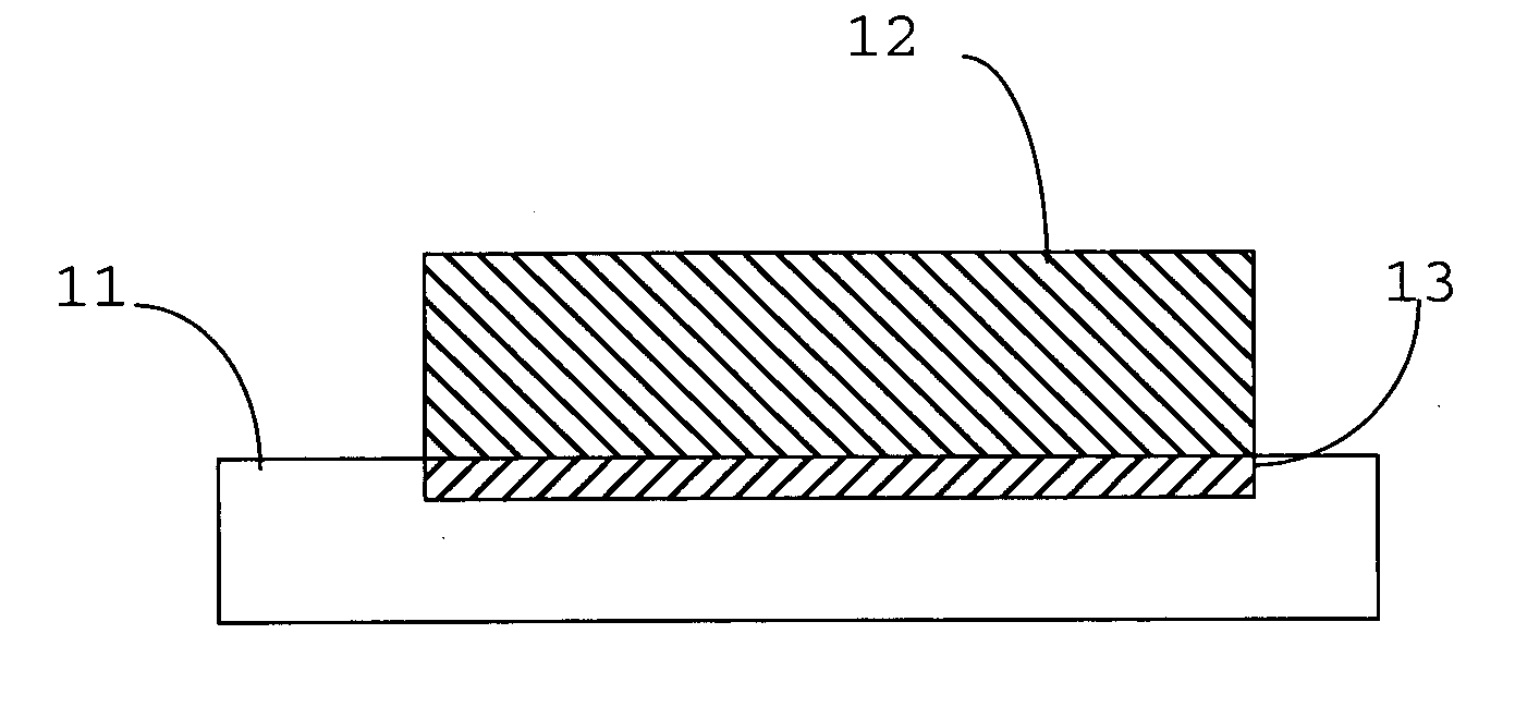
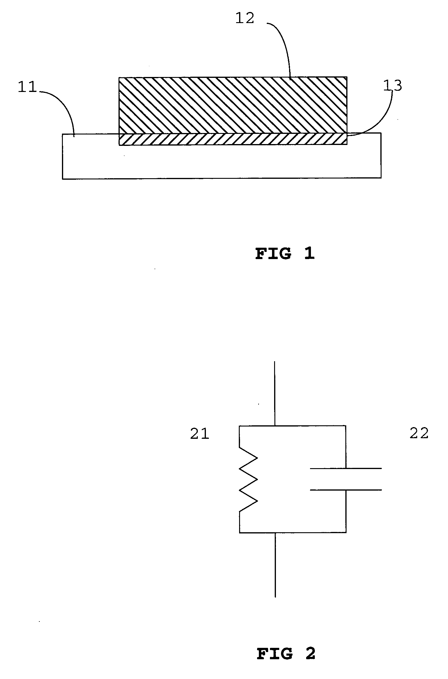
[0017] N-type sub-collector, n-type collector, p-type base, n-type emitter, and n-type emitter contact layers are formed on a semi-insulating GaAs wafer by conventional means, with the constraint that the top 50 to 200A of the base layer is doped between 8×10¹⁸ and 8×10¹⁹ / cm3 p-type.

[0018] The wafer is then processed to form an interdigitated npn HBT by using conventional means, or similarly, using the structure described in the patent application titled “Integrated anneal cap / ion implant mask / trench isolation structure for III-V devices (application number 10801431), until the base semiconductor is exposed.

[0019] The surface of the semiconductor is cleaned with an acid such as HCl, then tungsten is then deposited on the entire wafer using physical vapor deposition.

[0020] Photoresist is patterned over the tungsten using methods well known in the art.

[0021] The tungsten is etched using a fluorine-containing plasma into a pattern defined by the photoresist.

[0022] The photoresist ...

second embodiment

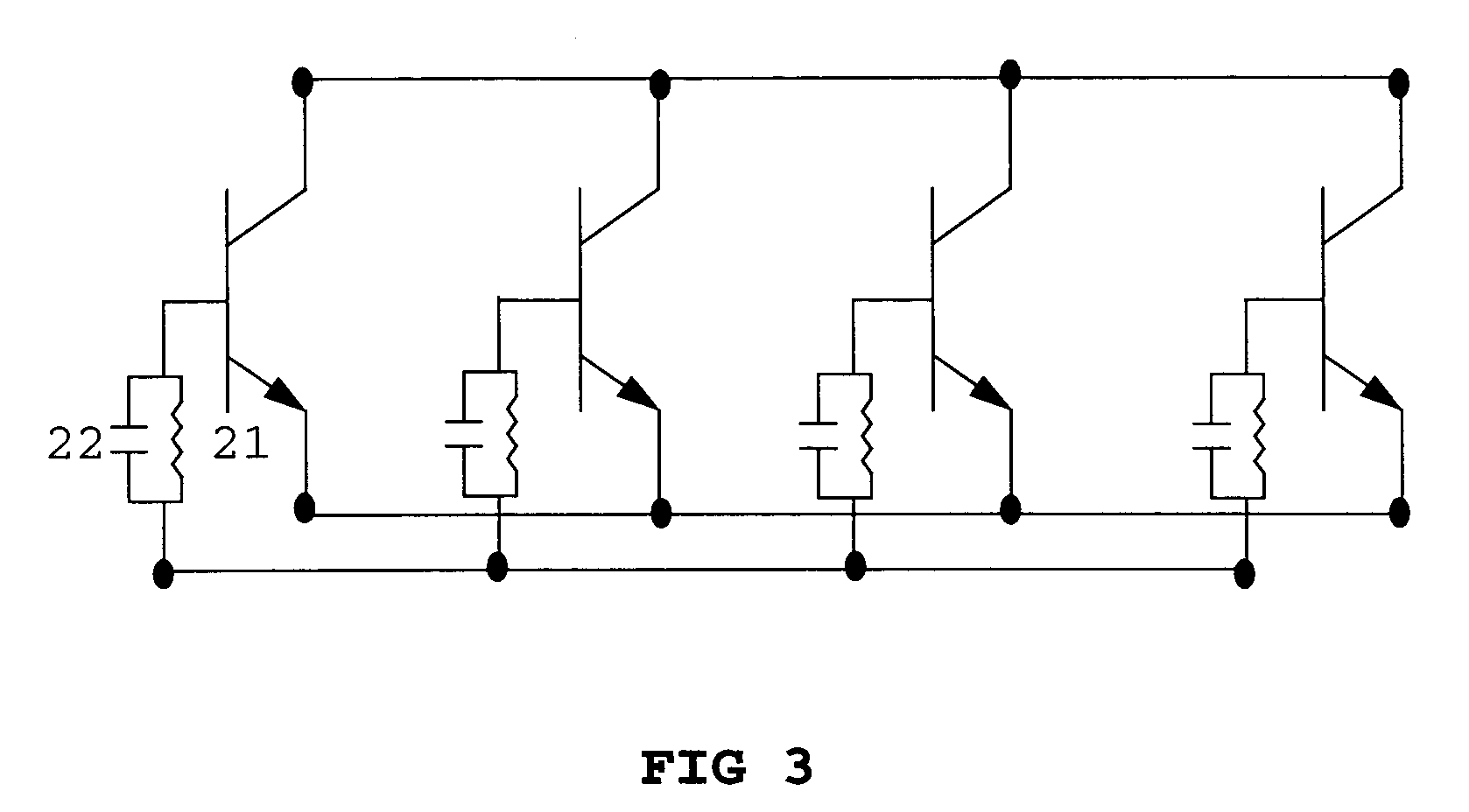
[0024] A interdigitated power n-channel field effect transistor is fabricated on GaAs up to the point of source contact by conventional means, except the source region is doped between 8×10¹⁸ and 8'1019 / cm3 n-type.

[0025] The surface of the semiconductor is cleaned with an acid such as HCl, then tungsten is deposited on the entire wafer using physical vapor deposition.

[0026] Photoresist is patterned over the tungsten using methods well known in the art.

[0027] The tungsten is etched using a fluorine-containing plasma into a pattern defined by the photoresist.

[0028] The photoresist is removed by methods well known in the art.

[0029] Optionally, a dielectric may be deposited over the newly patterned source contact metal, and annealed at an elevated temperature to sinter the contact. The temperature required for contact sinter must be high enough for the tungsten to absorb interfacial oxide between it and the semiconductor, but not high enough to damage the semiconductor (400-700 C)....


PUM


Abstract

A structure with the combined benefits of a highly reliable ohmic contact, ballast resistor, and ballast resistor bypass capacitor is provided. The benefit of these three features is combined into a single metal-semiconductor contact offering a reduction in space utilization, and complexity normally present in ballast networks associated with power devices.

Description

CROSS-REFERENCE TO RELATED APPLICATIONS [0001] Application number 10801431, Integrated anneal cap / ion implant mask / trench isolation structure for III-V devices. Referenced in detailed description section of this application. STATEMENT REGARDING FEDERALLY SPONSORED RESEARCH OR DEVELOPMENT [0002] This Invention was not conceived, constructed, or tested during the performance of a government contract. REFERENCE TO SEQUENCE LISTING, A TABLE, OR A COMPUTER PROGRAM LISTING COMPACT DISK APPENDIX [0003] Not Applicable BACKGROUND OF THE INVENTION [0004] 1. Field of Invention [0005] The present invention relates to semiconductor devices, such as power bipolar transistors, and power field effect transistors. [0006] 2. Description of the Prior Art [0007] Transistors used in power applications rely on ballast resistors to mitigate effects such as thermal run-away and current collapse. In bipolar junction transistors, ballast resistors are placed in series with either the emitter, base, and in so...

Claims


Application Information

Patent Timeline
Patent Type & Authority Applications(United States)
IPC IPC(8): H01L27/082
CPCH01L27/0605H01L27/0658H01L27/0802H01L27/0805
Inventor JOHNSON, DAVID A.
Owner JOHNSON DAVID A
Why Eureka
Try Eureka