MEMS device having contact and standoff bumps and related methods

a technology of microelectromechanical systems and bumps, which is applied in the direction of electrostatic motors, electrothermal relays, optical radiation measurement, etc., can solve the problems of structural deflection, extrinsic stresses in structural materials, and unwanted contact of electrode pairs

Inactive Publication Date: 2005-04-05
AAC TECH PTE LTD
View PDF9 Cites 180 Cited by
  • Summary
  • Abstract
  • Description
  • Claims
  • Application Information

AI Technical Summary

Benefits of technology

According to one embodiment, a movable MEMS component suspended over a substrate is provided. The component can include a structural layer having a movable electrode separated from a substrate by a gap. The component can also include at least one standoff bump attached to the structural layer and extending into the gap for preventing contact of the movable electrode with conductive material when the component moves.
According to a second embodiment, a MEMS device having standoff bumps is provided and can include a substrate having a stationary electrode and a first stationary contact. The device can also include a movable component suspended above the substrate. The movable component can include a structural layer having a movable electrode and a movable contact, wherein the movable electrode is spaced from the stationary electrode by a first gap and the movable contact is spaced from the first stationary contact by a second gap. The movable component can also include at least one standoff bump attached to the structural layer and extending into the first gap for preventing the contact of the movable electrode with the stationary electrode.
According to a sixth embodiment, a method for fabricating a movable, MEMS component having a standoff bump is provided. The method can include depositing a sacrificial layer on a conductive component and forming a movable electrode on the sacrificial layer for spacing the movable electrode and the conductive material by a gap upon the removal of the sacrificial layer. The method can also include forming a standoff bump in the sacrificial layer whereby the standoff bump extends into the gap between the movable electrode and the conductive component. Further, the method can include depositing a structural layer on the movable electrode and the standoff bump and removing the sacrificial layer to form a gap spacing the conductive component from the movable electrode whereby the standoff bump extends into the gap for preventing contact of the movable electrode with the conductive material when the component moves.

Problems solved by technology

One of the problems that faces current MEMS switches is unwanted contact of the electrode pair.
However, an unwanted contact of the electrodes can result from this design.
Other undesirable structural deflections usually result from intrinsic or extrinsic stresses in the structural materials.
A common undesirable structural deflection due to extrinsic stress occurs over temperature in composite structures comprised of two or more materials with different Coefficients of Thermal Expansion (CTE).
It is undesirable for the electrodes to touch because an electrical short between the electrodes can result.
Thus, such a design requires greater power consumption and possibly additional electrical components to achieve higher actuation voltages.

Method used


Image

  • MEMS device having contact and standoff bumps and related methods
  • MEMS device having contact and standoff bumps and related methods
  • MEMS device having contact and standoff bumps and related methods

Examples


Embodiment Construction

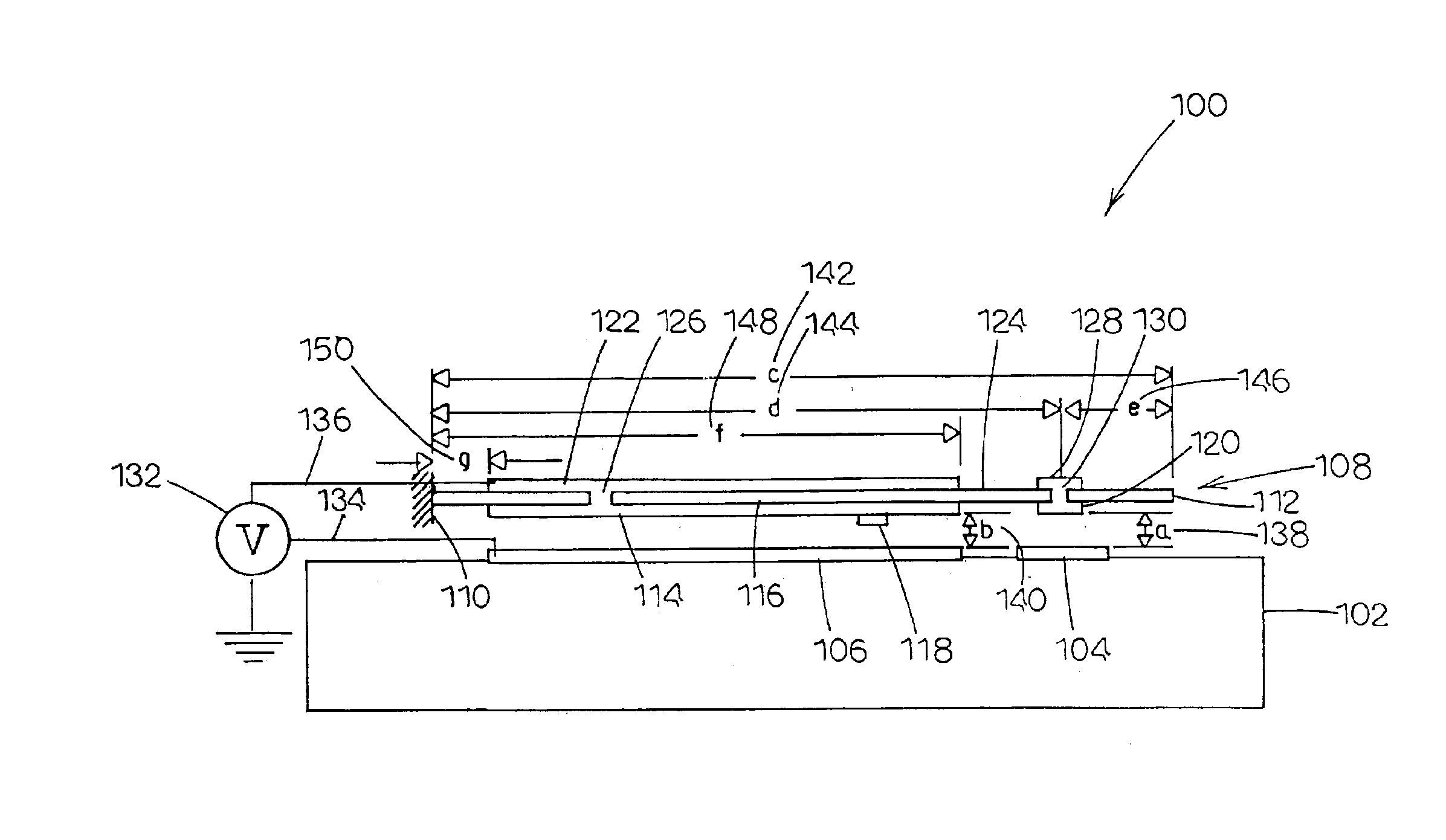
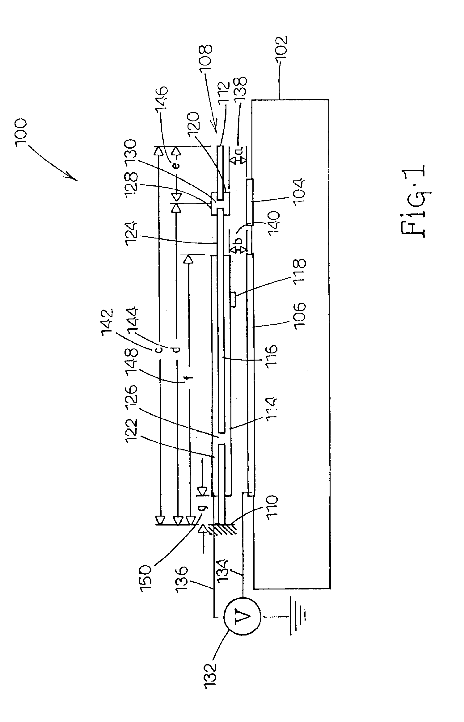
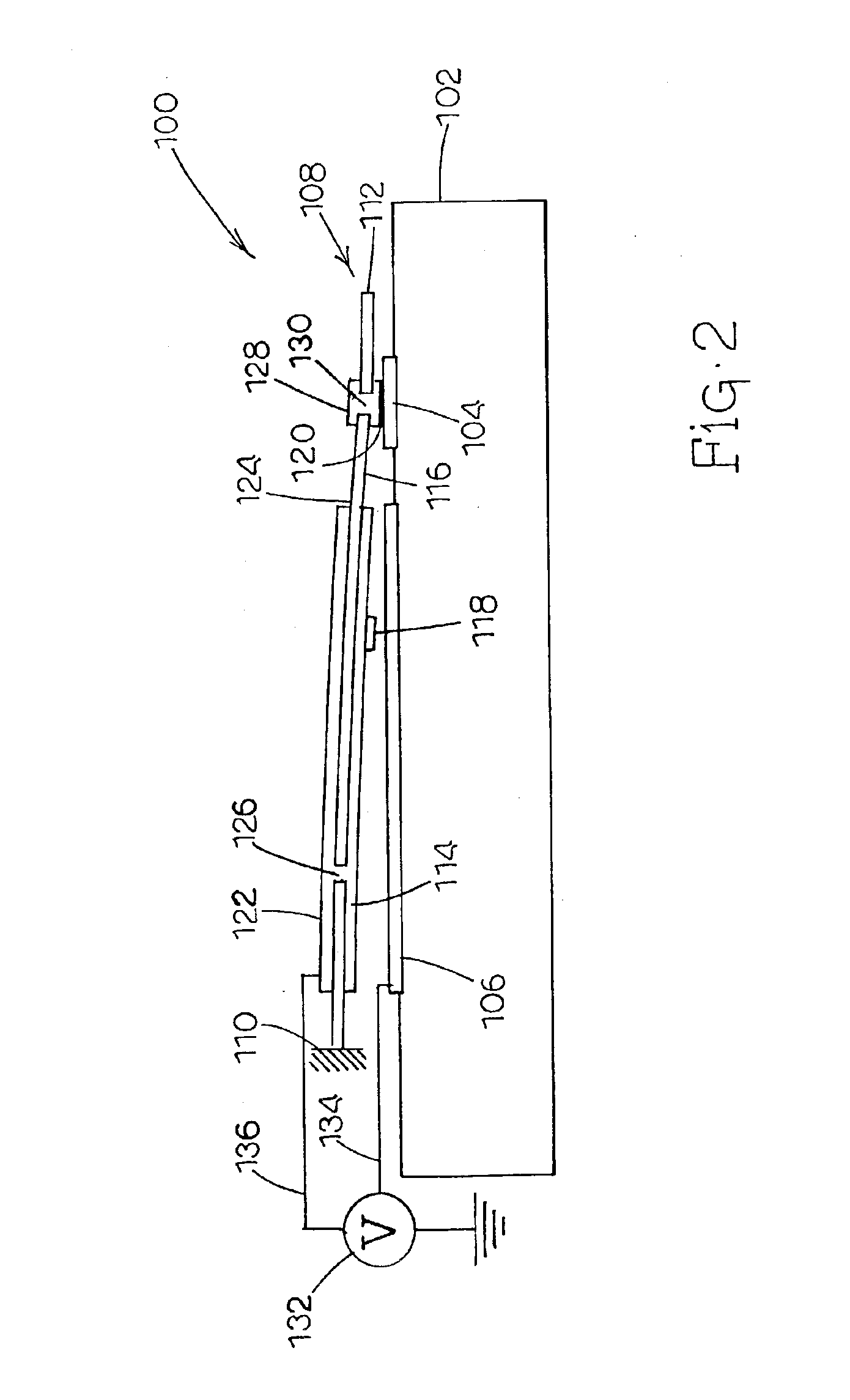
For purposes of the description herein, it is understood that when a component such as a layer or substrate is referred to herein as being deposited or formed “on” another component, that component can be directly on the other component or, alternatively, intervening components (for example, one or more buffer or transition layers, interlayers, electrodes or contacts) can also be present. Furthermore, it is understood that the terms “disposed on” and “formed on” are used interchangeably to describe how a given component can be positioned or situated in relation to another component. Therefore, it will be understood that the terms “disposed on” and “formed on” do not introduce any limitations relating to particular methods of material transport, deposition, or fabrication.

Contacts, interconnects, conductive vias, and electrodes of various metals can be formed by sputtering, CVD, or evaporation. If gold, nickel or PERMALLOY™ (NixFey) is employed as the metal element, an electroplating...


PUM

PropertyMeasurementUnit
temperatureaaaaaaaaaa
lengthaaaaaaaaaa

Abstract

MEMS Device Having Contact and Standoff Bumps and Related Methods. According to one embodiment, a movable MEMS component suspended over a substrate is provided. The component can include a structural layer having a movable electrode separated from a substrate by a gap. The component can also include at least one standoff bump attached to the structural layer and extending into the gap for preventing contact of the movable electrode with conductive material when the component moves.

Description

TECHNICAL FIELDThe present invention generally relates to micro-electro-mechanical systems (MEMS) devices and methods. More particularly, the present invention relates to the design and fabrication of a MEMS device having contact and standoff bumps and related methods.BACKGROUND ARTAn electrostatic MEMS switch is a switch operated by an electrostatic charge and manufactured using micro-electro-mechanical systems (MEMS) techniques. A MEMS switch can control electrical, mechanical, or optical signal flow. MEMS switches have typical application to telecommunications, such as DSL switch matrices and cell phones, Automated Testing Equipment (ATE), and other systems that require low cost switches or low-cost, high-density arrays.As can be appreciated by persons skilled in the art, many types of MEMS switches and related devices can be fabricated by either bulk or surface micromachining techniques. Bulk micromachining generally involves sculpting one or more sides of a substrate to form de...

Claims


Application Information

Patent Timeline
Patent Type & Authority Patents(United States)
IPC IPC(8): H01H61/00H01H59/00H01H61/04H02N10/00H01H1/50H01H1/02H01H1/00H01H1/04H01L27/12B81B3/00B81B7/00H01L21/302H01L23/373H01L23/522H01L29/86H02N1/00
CPCB81B3/0024B81C1/0015H01H59/0009H01H61/04H01L23/3735H01L23/522H02N1/006H02N10/00B81B3/0051Y10T29/49222B81B2201/014B81B2201/018B81B2203/0118B81B2203/04B81B2207/07B81C2201/0107B81C2201/0108B81C2201/0109H01H1/04H01H1/504H01H2001/0042H01H2001/0063H01H2001/0089H01H2059/0072H01H2061/006H01L27/1203H01L2924/09701H01L2924/0002H01L2924/00
Inventor DEREUS, DANA RICHARD
Owner AAC TECH PTE LTD
Why Eureka
Try Eureka