
Semiconductor integrated circuit

Inactive Publication Date: 2005-04-12
RENESAS ELECTRONICS CORP
View PDF6 Cites 31 Cited by
  • Summary
  • Abstract
  • Description
  • Claims
  • Application Information

AI Technical Summary

Benefits of technology

It is therefore an object of the present invention to provide a semiconductor integrated circuit that can deliver stable oscillation frequencies when employed for voltage controlled oscillators while providing for a reduced area occupied by inductors.
The present invention employs the inductors formed of at least two electrically conductive layers, thereby providing a further reduced area occupied by the inductors when compared with inductors formed of only one conductive layer. Furthermore, since the contents of the electrically conductive layers in the two inductors are equal to each other, both the inductors are equally subjected to external disturbances such as parasitic capacitance. This makes the inductors impervious to a property mismatch therebetween and allows for providing stable oscillation frequencies. The inductors need not always to be connected directly to two power supply lines, and a transistor or the like may be provided between the inductors and the power supply lines.
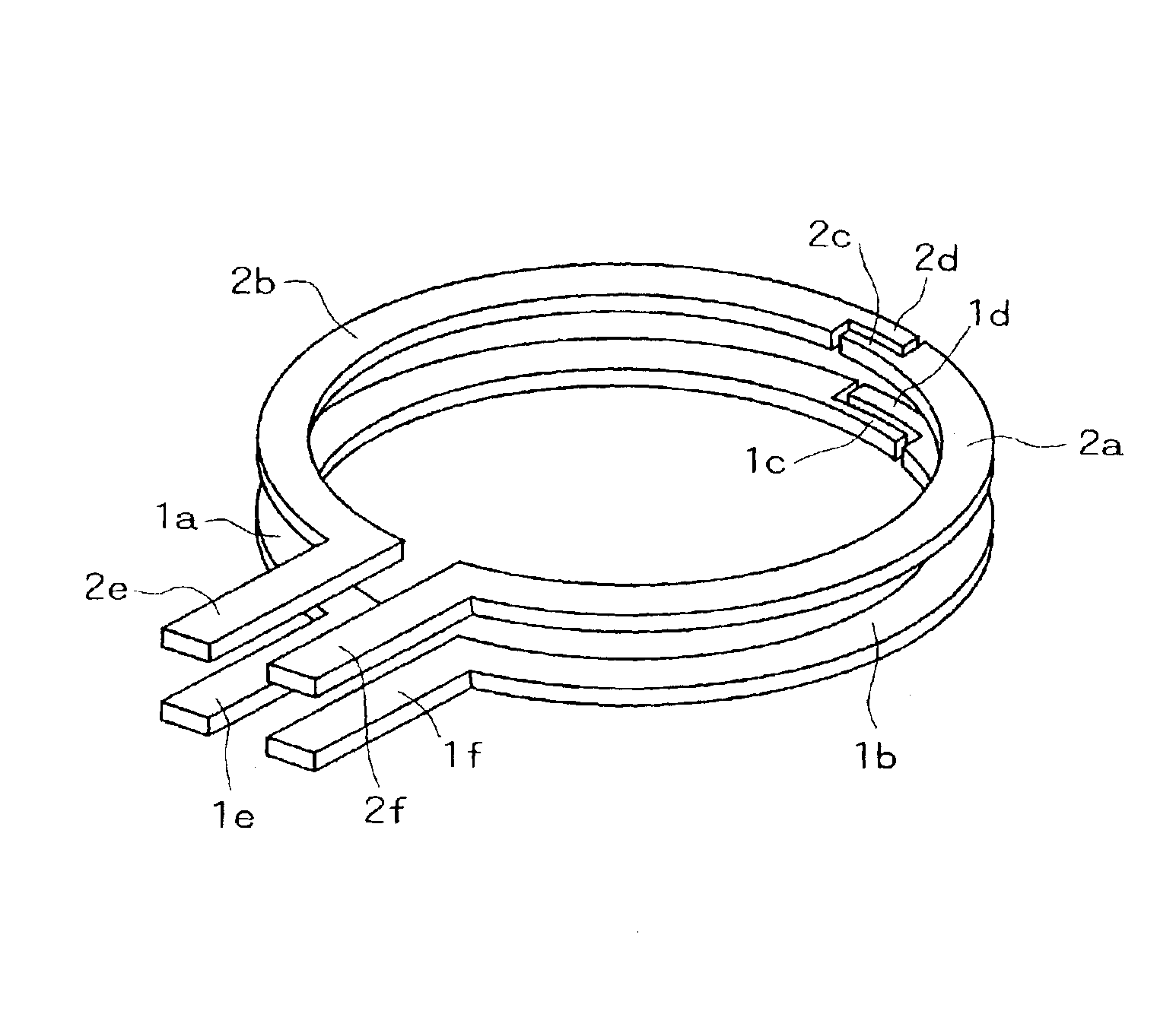
The two inductors can have two electrically conductive layers, and the ratio of a length of a lower electrically conductive layer and the ratio of a length of an upper electrically conductive layer to the total length of an electrically conductive layer constituting each conductor can be made equal to each other. This makes it possible to reduce the area occupied by the inductors to half the area occupied by inductors formed of only one layer.
Furthermore, one of the two inductors may be provided with two first upper electrically conductive layers formed on the same interlayer insulating film and having both end portions spaced apart from each other, and a first lower electrically conductive layer underlying the first upper electrically conductive layers and having an end portion overlapping with the end portion of the two first upper electrically conductive layers in a plan view. The other of the two inductors may also be provided with two second upper electrically conductive layers formed on the same interlayer insulating film as the first upper electrically conductive layers, being the same in total length as the first upper electrically conductive layer, and having both end portions spaced apart from each other; and a second lower electrically conductive layer underlying the second upper electrically conductive layers and having an end portion overlapping with the end portion of the two second upper electrically conductive layers in a plan view. Thus, the two inductors are configured to intersect each other in a plan view. This makes it possible to increase the content of the first and second upper electrically conductive layers in each inductor, and provide higher Q values with increasing contents of an electrically conductive layer spaced apart from the semiconductor substrate.
Furthermore, the at least two electrically conductive layers can be connected to each other via a contact. In this case, the electrically conductive layers can be made wider at a region where the contact is provided than at other portions, thereby preventing an increase in electrical resistance caused by the contact provided.

Problems solved by technology

Furthermore, since the contents of the electrically conductive layers in the two inductors are equal to each other, both the inductors are equally subjected to external disturbances such as parasitic capacitance.

Method used


Image

  • Semiconductor integrated circuit
  • Semiconductor integrated circuit
  • Semiconductor integrated circuit

Examples


first embodiment

Now, the present invention will be described below more specifically with reference to the accompanying drawings in accordance with the embodiments. FIG. 5 is a schematic view illustrating a semiconductor integrated circuit according to the present invention.

FIG. 6 is a schematic view illustrating a connection between inductors according to the first embodiment.

FIG. 7 is a cross-sectional view taken along the line A—A of FIG. 6.

In the first embodiment, there are formed an interlayer insulating film 11 on a semiconductor substrate 10, and semicircular electrically conductive layers 1a and 1b on the interlayer insulating film 11. For example, the conductive layers 1a and 1b are formed so as to form part of the same circle. In other words, the center of one circle having the conductive layer 1a as a semicircle is aligned with the center of the other circle having the conductive layer 1b as a semicircle, with these circles being equal to each other in radius. For example, the conductive...

second embodiment

Now, the present invention will be explained below with reference to a

FIGS. 10 and 11 are a schematic view and a plan view illustrating a semiconductor integrated circuit according to the second embodiment of the present invention, respectively.

In the second embodiment, first and second interlayer insulating films (not shown) are successively deposited on a semiconductor substrate (not shown), and then a semicircular conductive layers 3a and 3b are formed thereon. For example, the conductive layers 3a and 3b are formed so as to constitute part of the same circle. In other words, the center of one circle having the conductive layer 3a as a semicircle is aligned with the center of the other circle having the conductive layer 3b as a semicircle, and these circles are equal to each other in radius. For example, the conductive layers 3a and 3b have a width of a few nm to a few tens of nm, and the circles having these layers as a semicircle have, but not limited to, a radius of the order ...


PUM


Abstract

Electrically conductive layers 1a and 2a connected to each other via a contact form one inductor, while electrically conductive layers 1b and 2b connected to each other via other contact form the other inductor. Since the areas defined by the loops forming these two inductors are equal to each other, the inductances of the inductors are also equal to each other. Between both the inductors, the lengths in the loop of the portions (the conductive layers 1a and 1b) formed on a lower interlayer insulating film are equal to each other, while the lengths in the loop of the portions (the conductive layers 2a and 2b) formed on an upper interlayer insulating film are also equal to each other. This allows external disturbances such as parasitic capacitance to affect both the inductors equally. Accordingly, a voltage controlled oscillator incorporating the invention can stably provide undistorted sinusoidal oscillation signals.

Description

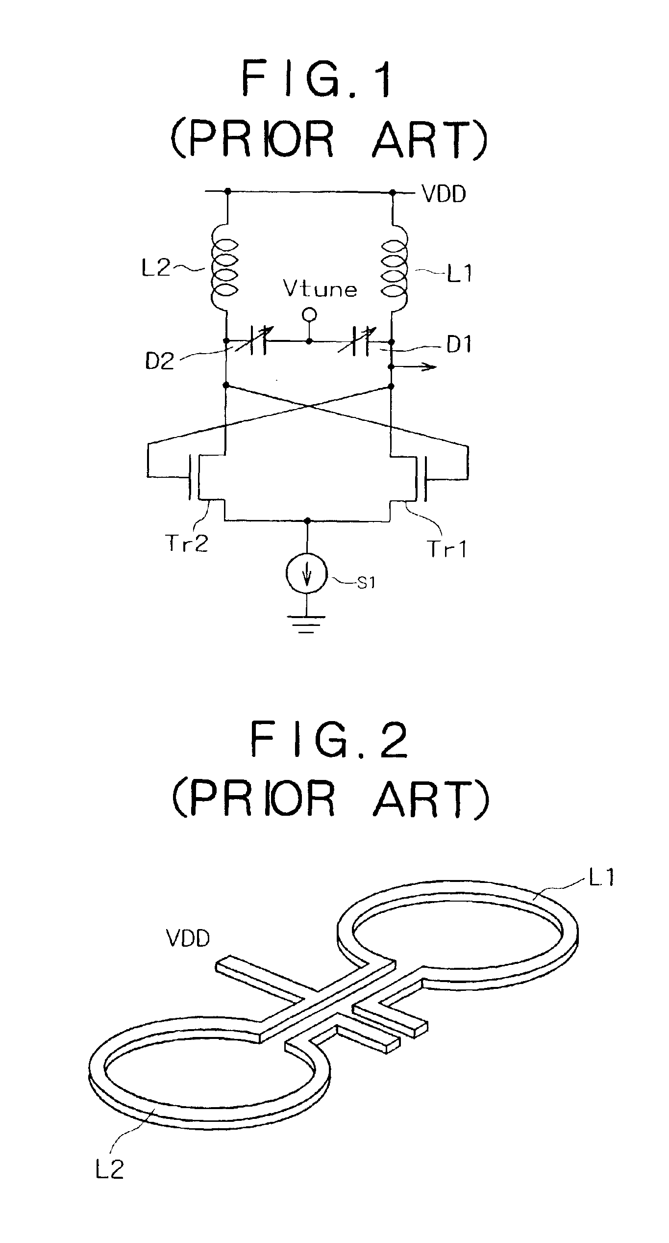
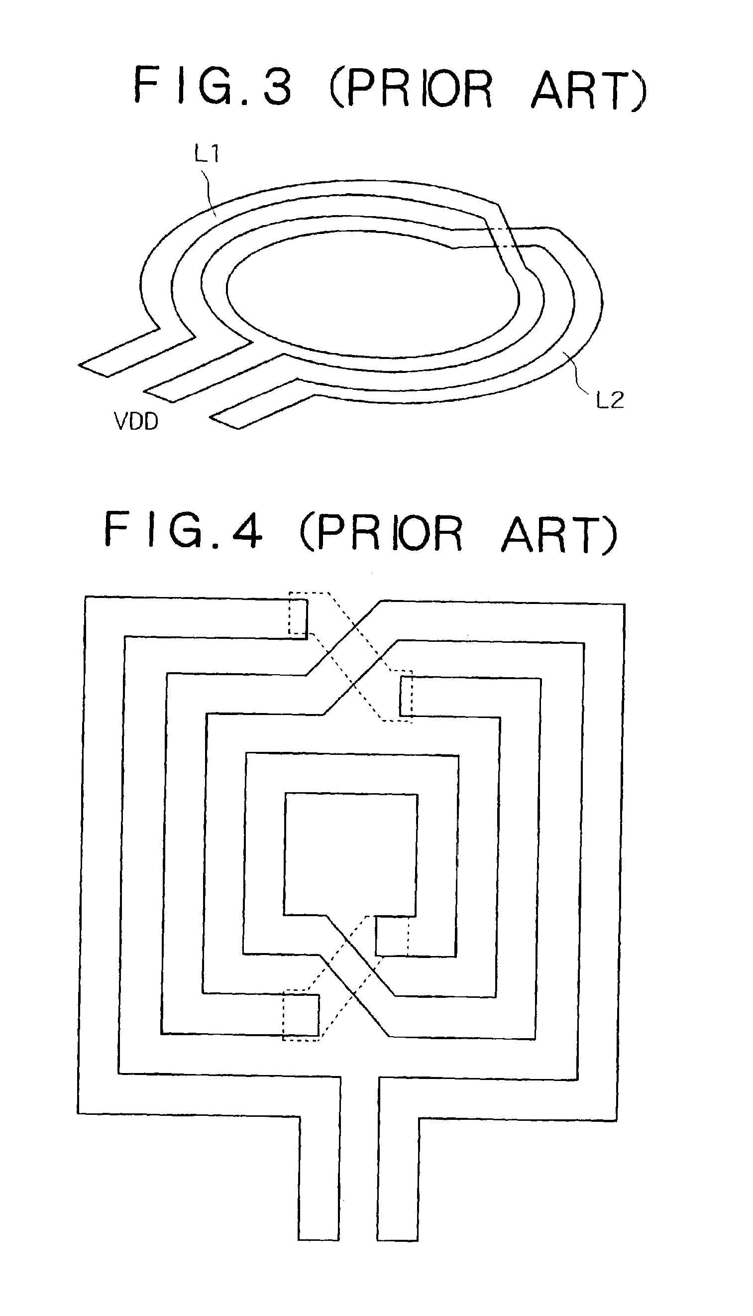
BACKGROUND OF THE INVENTION1. Field of the InventionThe present invention relates to semiconductor integrated circuits suitable for use in voltage controlled oscillators and more particularly to a semiconductor integrated circuit that can deliver stable oscillation frequencies while providing for a reduced area occupied by inductors.2. Description of the Related ArtConventionally, a voltage controlled oscillator (VCO) has been available that is built in high-frequency semiconductor devices or the like. FIG. 1 is a circuit diagram illustrating a prior art voltage controlled oscillator.In the prior art voltage controlled oscillator, the drains of transistors Tr1 and Tr2 are connected to a constant current power supply S1. Inductors L1 and L2 are each connected at one end thereof to a power supply line through which a power supply voltage VDD is provided. The inductance of the inductor L1 is equal to that of the inductor L2. On the other hand, the inductor L1 is connected at the other ...

Claims


Application Information

Patent Timeline
IPC IPC(8): H01L27/08H03B5/08H03B5/12H01F17/00H01F17/02H01L21/822H01L27/04
CPCH03B5/124H03B5/1228H03B5/1215H01L27/08H01F17/0006H01F2021/125H01L27/02
Inventor FURUMIYA, MASAYUKIYAMAMOTO, RYOTAKISHI, JUNOHKUBO, HIROAKINAKASHIBA, YASUTAKA
Owner RENESAS ELECTRONICS CORP
Learn More