Memory device test system and method

a memory device and test system technology, applied in the field of test apparatuses, can solve the problems of failures at or near the upper operational frequency limits of the device, similar 64 mbit memory devices cannot be tested at speed, and the incremental testing process to take a relatively long time, so as to achieve the effect of significantly reducing the test tim

Inactive Publication Date: 2005-04-12
MACRONIX INT CO LTD
View PDF5 Cites 45 Cited by
  • Summary
  • Abstract
  • Description
  • Claims
  • Application Information

AI Technical Summary

Benefits of technology

The inventive testing system can reduce the above-described DBM capacity problem, as can the inventive method for testing a memory device. Relatively large memory devices, which would otherwise require multiple passes to be completely tested, can be tested “at speed” in a single pass. As a result, testing time can be significantly reduced.

Problems solved by technology

Some possible defects of memory devices only become apparent (i.e., result in faults) at or near upper operational frequency limits of the devices.
However, a similar 64 Mbit memory device cannot be tested “at speed” in a single pass.
This incremental testing process is undesirable in that necessary delays between each testing pass can be cumulative, causing the incremental testing process to take a relatively long time.

Method used


Image

  • Memory device test system and method
  • Memory device test system and method
  • Memory device test system and method

Examples


Embodiment Construction

Reference will now be made in detail to the presently preferred embodiments of the invention, examples of which are illustrated in the accompanying drawings. Wherever possible, the same or similar reference numbers are used in the drawings and the description to refer to the same or like parts. It should be noted that the drawings are in simplified form and are not to precise scale.

Although the disclosure herein refers to certain illustrated embodiments, it is to be understood that these embodiments are presented by way of example and not by way of limitation. The intent of the following detailed description, although discussing exemplary embodiments, is to be construed to cover all modifications, alternatives, and equivalents of those embodiments as may fall within the spirit and scope of the invention as defined by the appended claims.

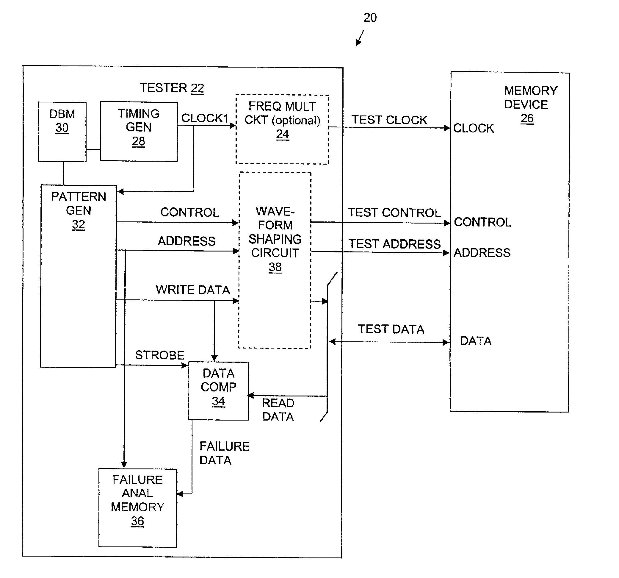
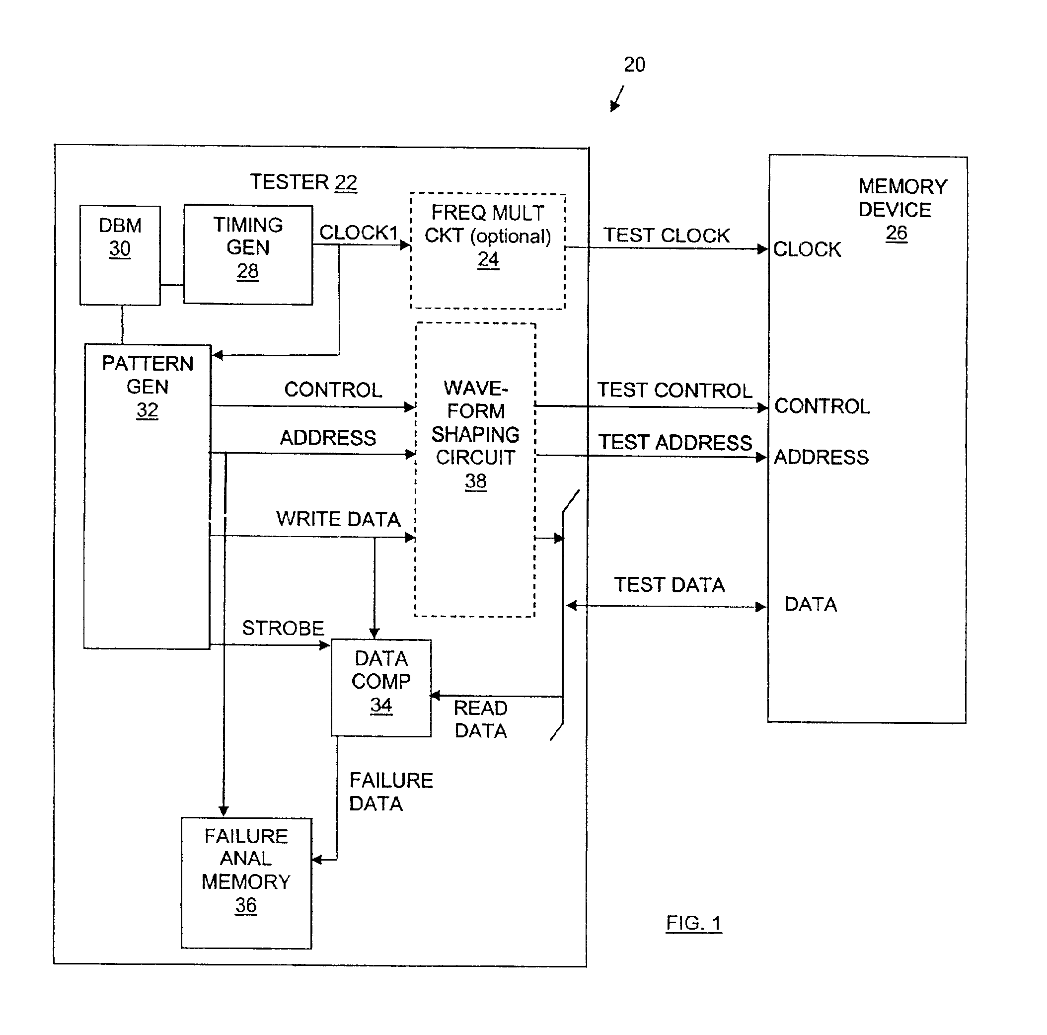
Referring more particularly to the drawings, FIG. 1 is a diagram of one embodiment of a testing system 20 applied to a memory device 26 under test. ...


PUM


Abstract

A testing system is described for testing a memory device. The testing system includes a timing generator, an optional frequency multiplier circuit, a pattern generator, and a waveform shaping circuit. The timing generator generates a first clock signal. The frequency multiplier circuit receives the first clock signal, and uses the first clock signal to produce a second clock signal. In general, the second clock signal has a frequency greater than a frequency of the first clock signal. The frequency of the second clock signal may twice the frequency of the first clock signal. The testing system provides the second clock signal to the memory device such that operations within the memory device are synchronized to the second clock signal. The waveform shaping circuit produces an address signal synchronized to the first clock signal, and provides the address signal to the memory device when reading data from the memory device. In another embodiment, the first clock signal is not used and the address signals are synchronized to every two cycles of the second clock signal. A method for testing a memory device, which may be embodied in the testing system, is also described.

Description

BACKGROUND OF THE INVENTION1. Field of the InventionThe present invention relates generally to testing apparatuses and, more particularly, to systems for testing memory devices and methods of using the systems.2. Description of Related ArtInternal operations of synchronous memory devices, such as synchronous mask read only memory (ROM) devices and synchronous dynamic random access memory (SDRAM) devices, are typically synchronized to a single external clock signal. Such a clock signal synchronization feature can eliminates the need to comply with complex timing requirements of multiple timing strobes typical of asynchronous memory devices. In addition, the memory cells of a typical SDRAM device, for example, are arranged in multiple arrays called banks, instead of as a single array. While one of the banks is being accessed, one or more of the other banks may be readied for subsequent access (e.g., signal lines of the one or more other banks may be precharged). This essentially allow...

Claims


Application Information

Patent Timeline
Patent Type & Authority Patents(United States)
IPC IPC(8): G11C29/56
CPCG11C29/56G11C29/56012G11C2029/5606
Inventor LIN, WEN-HSITSENG, CHIN-CHUNG
Owner MACRONIX INT CO LTD
Why Eureka
Try Eureka