SAR analog-to-digital converter with two single ended inputs

an analog-to-digital converter and input technology, applied in the field of data converters, can solve problems such as errors and weighting of capacitor arrays

Inactive Publication Date: 2005-04-19
SILICON LAB INC
View PDF14 Cites 25 Cited by
  • Summary
  • Abstract
  • Description
  • Claims
  • Application Information

AI Technical Summary

Benefits of technology

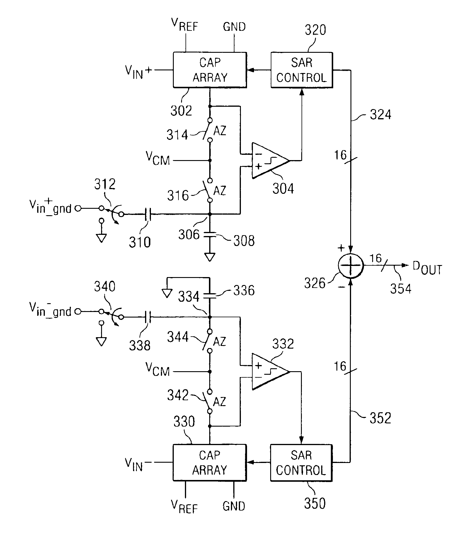
[0008]FIG. 3 illustrates a higher level view of the

Problems solved by technology

A number of problems exist with the data conversion of an analog signal to a digital signal.
Some of these problems reside in the various offsets of the inputs to the comparators, one of which is due to the fact that the actual chip ground may be different from the input ground at the PC board on which the actual chip is disposed.
Additional

Method used


Image

  • SAR analog-to-digital converter with two single ended inputs
  • SAR analog-to-digital converter with two single ended inputs
  • SAR analog-to-digital converter with two single ended inputs

Examples


Embodiment Construction

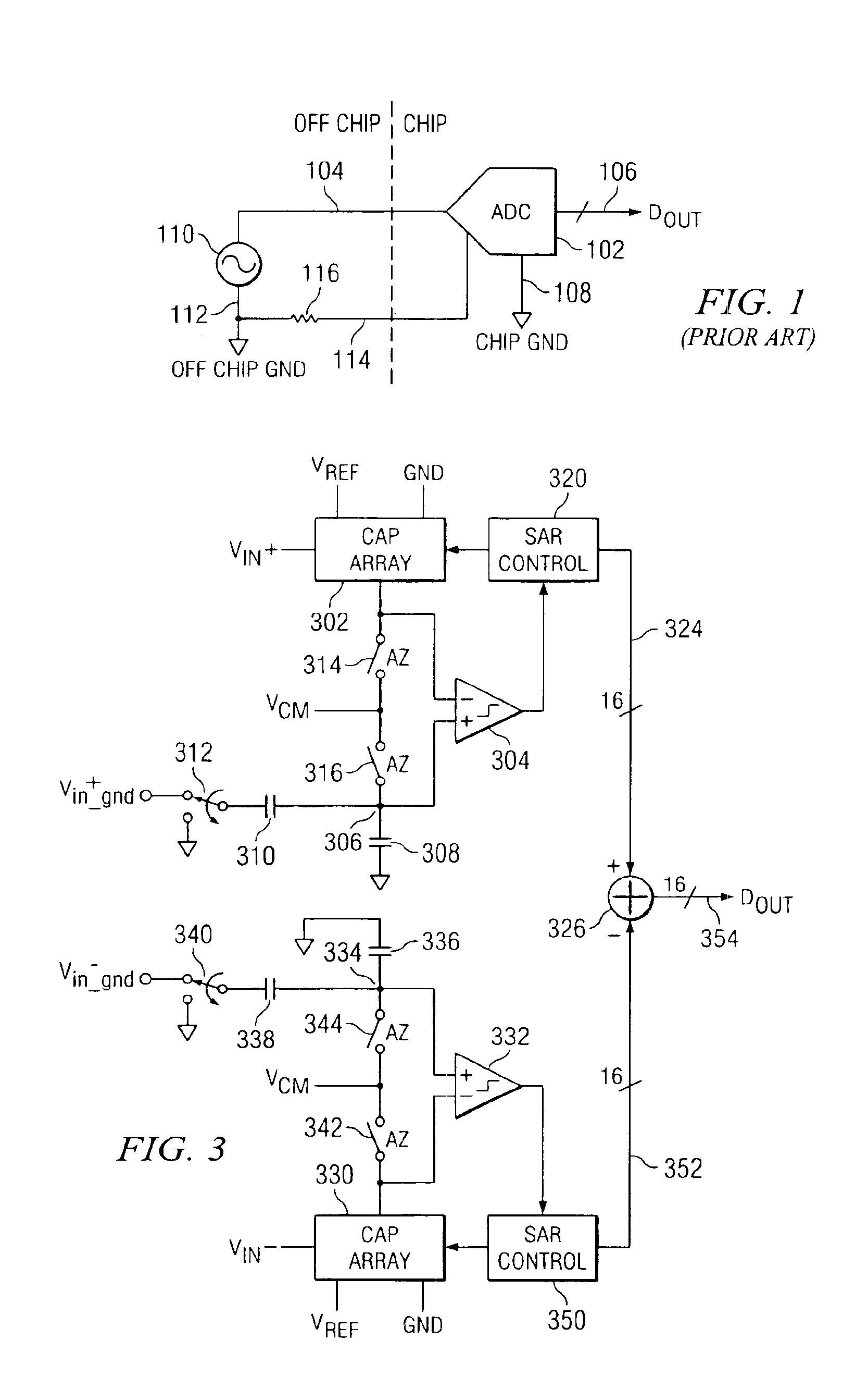
[0022]Referring now to FIG. 1, there is illustrated a diagrammatic view of an analog-to-digital convertor (ADC) 102 that is represented by a conventional ADC symbol. This ADC 102 has an analog input 104 and a digital output 106. Additionally, it is noted that ADC 102 is typically fabricated on a chip or on a PC board. Associated with the ADC 102 is a chip ground 108 that is the ground connection to the ADC 102 in proximity thereto. However, the input voltage on line 104 typically is derived from some type of external voltage source 110. Associated with that voltage source 110 is an off chip ground 112 or an off board ground. This ground is typically connected to the ADC 102 through a ground line 114, this ground line 114 having associated therewith a finite resistivity or resistance 116. As such, the voltage of the off chip ground 112 may actually be different than the chip ground 108. As will be described hereinbelow, this resistance offset in the voltage between the off chip groun...


PUM


Abstract

Self calibrating SAR analog-to-digital converter. A data converter for converting analog data on a differential data input having a positive analog input terminal and a negative analog input terminal to digital data. The data converter includes a first single ended successive approximation register (SAR) analog-to-digital converter for converting the analog signal on the positive analog input terminal to a first digital signal and a second single ended successive approximation register (SAR) analog-to-digital converter for converting the analog signal on the negative analog input terminal to a second digital signal. A circuit for combining the first and second digital signals as a digital output signal for the data converter that represents the difference between the analog signals on the positive and negative analog input terminals.

Description

TECHNICAL FIELD OF THE INVENTION[0001]The present invention pertains in general to data converters and, more particularly, to analog-to-digital converters.BACKGROUND OF THE INVENTION[0002]Data converters are provided for receiving either an analog signal for conversion to a digital signal or a digital signal for conversion to analog signal. For conversion of analog signals to digital signals, an analog-to-digital converter is utilized. This is typically facilitated by sampling an analog voltage onto a capacitor array having a plurality of binary weighted capacitors. The capacitors then have the ability to have one plate thereof selectively switched between a reference voltage and ground to redistribute the charge among the capacitors, the switching done in a sequential manner in accordance with a successive approximation algorithm. By selectively switching the plates of the capacitors, and comparing the other plate of the capacitors, which is connected to a common input of a compara...

Claims


Application Information

Patent Timeline
IPC IPC(8): G06F13/20G06F13/28H01C10/00H01C10/16H03M1/06H03M1/38H03M1/12H03M1/66H03M1/34H03M1/10H03M1/78H03M1/74H03M1/46
CPCH03M1/1057H03M1/468
Inventor LEUNG, KA Y.LEUNG, KAFAI
Owner SILICON LAB INC
Why Eureka
Try Eureka