Light modulation medium and light modulation method

Inactive Publication Date: 2005-04-19
FUJIFILM BUSINESS INNOVATION CORP
View PDF3 Cites 5 Cited by
  • Summary
  • Abstract
  • Description
  • Claims
  • Application Information

AI Technical Summary

Benefits of technology

[0020]Because a light modulation medium according to the invention has a light modulation element formed by arranging plural light modulation layers and showing a wide margin of operation, it is possible to clearly change the liquid crystal orientation of each of the light modulation layers by applying various voltages between the electrodes and cause the light modulation medium to display clear color tones

Problems solved by technology

Consumption of large volumes of paper has been a serious problem of modern societies because it leads to destructions of forest resources that supply raw materials of paper pulps and environmental pollutions due to dumping and burning of paper wastes.
However, due to the development of information society that involves dissemination of personal computers and a wide use of the I

Method used


Image

  • Light modulation medium and light modulation method
  • Light modulation medium and light modulation method
  • Light modulation medium and light modulation method

Examples


1st embodiment

(1st Embodiment)

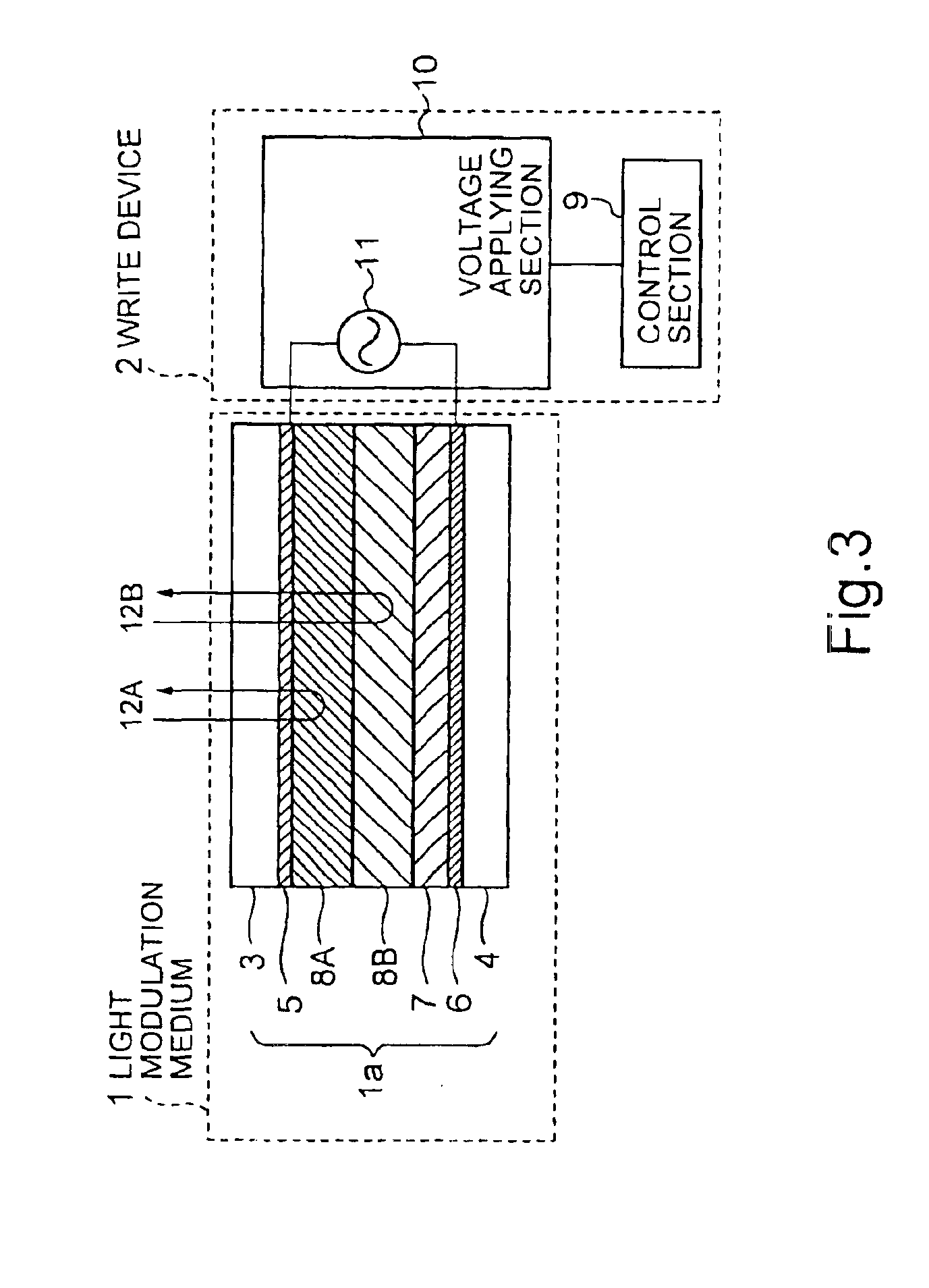
[0079]FIG. 3 schematically illustrates the first embodiment of light modulation medium and light modulation method along with a write device adapted to be used with the embodiment.

[0080]A light modulation medium 1 of FIG. 3 is formed by a light modulation element 1a that is by turn formed by arranging a light modulation layer 8A adapted to reflect a beam of read light 12A, a light modulation layer 8B adapted to reflect a beam of read light 12B and a light absorption layer 7 between a pair of substrates 3, 4 respectively carrying electrodes 5, 6 that are formed on the inner surfaces thereof. Thus, the light modulation medium 1 has a multilayer structure.

[0081]A write device 2 that is used for this embodiment of light modulation method has a voltage applying section 10 that applies a bias voltage 11 between the electrodes 5, 6 of the light modulation medium 1 and a control section 9 that controls the voltage applying section 10 according to the light modulation pattern...

2nd embodiment

(2nd Embodiment)

[0126]FIG. 12 schematically illustrates the second embodiment of light modulation medium and light modulation method along with a write device adapted to be used with the embodiment.

[0127]The light modulation medium 1 of FIG. 12 is formed by a light modulation element 1a that is by turn formed by arranging a light modulation layer 8A adapted to reflect a beam of read light 12A, a light modulation layer 8B adapted to reflect a beam of read light 12B, a light modulation layer 8C adapted to reflect a beam of read light 12C, a light absorption layer 7 and a photoconductive layer 13 between a pair of substrates 3, 4 respectively carrying electrodes 5, 6 that are formed on the inner surfaces thereof. Thus, the light modulation medium 1 has a multilayer structure.

[0128]Write device 2 that is used for this embodiment of light modulation method has a voltage applying section 10 that applies a bias voltage 11 between the electrodes 5, 6 of the light modulation medium 1, a ligh...

3rd embodiment

(3rd Embodiment)

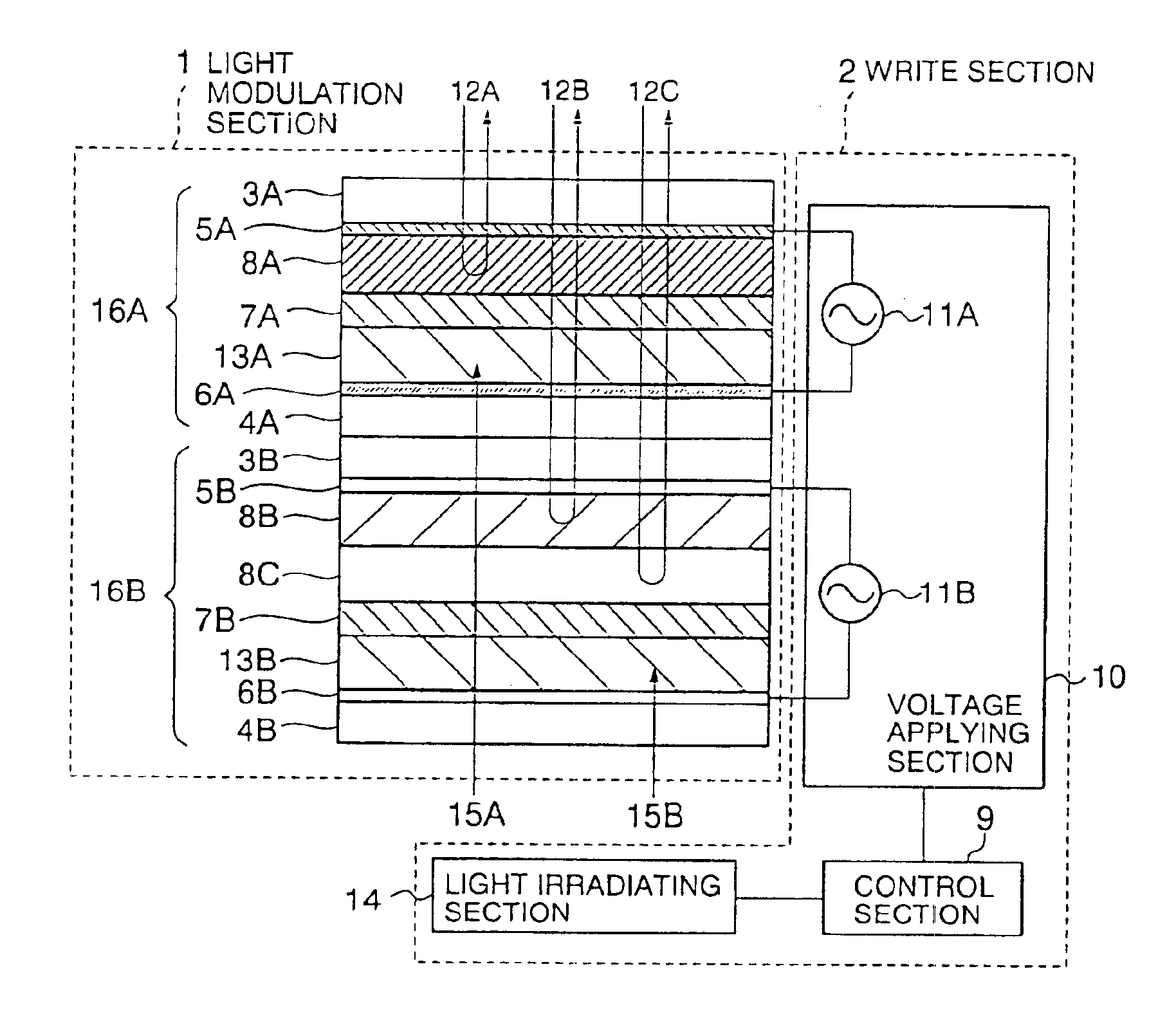
[0187]FIG. 20 schematically illustrates the third embodiment of light modulation medium and light modulation method along with a write device adapted to be used with the embodiment.

[0188]The light modulation medium 1 of FIG. 20 has two light modulation elements 16A and 16B. The light modulation element 16A is formed by arranging a light modulation layer 8A adapted to reflect a beam of read light 12A, a light absorption layer 7A and a photoconductive layer 13A between a pair of substrates 3A, 4A respectively carrying bias electrodes 5A, 6A that are formed on the inner surfaces thereof. On the other hand, the light modulation element 16B is formed by arranging a light modulation layer 8B adapted to reflect a beam of read light 12B, a light modulation layer 8C adapted to reflect a beam of read light 12C, a light absorption layer 7B and a photoconductive layer 13B between a pair of substrates 3B, 4B respectively carrying electrodes 5B, 6B that are formed on the inner sur...


PUM


Abstract

A light modulation medium comprises a light modulation element having a pair of substrates and plural light modulation layers arranged between the substrates to form a multilayer structure and made of cholesteric liquid crystal adapted to change the liquid crystal orientation in response to application of a predetermined electric field, in which the ratio of the threshold electric field at which the liquid crystal orientation is moved from a planar state to a focal conic state of a first light modulation layer of the light modulation element to that of a second light modulation layer is not less than 0.3 and the ratio of the dielectric constant in a planar state of liquid crystal orientation of the first light modulation layer to that of the second light modulation layer is not less than 4.

Description

BACKGROUND OF THE INVENTION[0001]1. Field of the Invention[0002]This invention relates to a light modulation medium having a light modulation element formed by laying plural light modulation layers to realize a multilayer structure and adapted to change the optical characteristic of each of the light modulation layers by controlling the electric field applied to the light modulation element and also to a light modulation method to be used with such a light modulation medium.[0003]2. Description of the Related Art[0004]Consumption of large volumes of paper has been a serious problem of modern societies because it leads to destructions of forest resources that supply raw materials of paper pulps and environmental pollutions due to dumping and burning of paper wastes. However, due to the development of information society that involves dissemination of personal computers and a wide use of the Internet, paper is being consumed at an increasing rate particularly as short-life documents t...

Claims


Application Information

Patent Timeline
IPC IPC(8): G02F1/13G02F1/137G02F1/1347G02F1/139G02F1/133G09G3/36
CPCG02F1/13476G09G3/3607G02F1/13718G02F2203/34
Inventor HARADA, HARUOARISAWA, HIROSHI
Owner FUJIFILM BUSINESS INNOVATION CORP
Why Eureka
Try Eureka