Frequency dividing circuit, power supply circuit and display device

a technology of power supply circuit and frequency dividing circuit, which is applied in the direction of oscillator, pulse technique, instruments, etc., can solve the problems of reducing the operating margin of the frequency dividing circuit as a whole, low current driving capability of the transistor formed by a low-temperature polysilicon process, and not following a high-frequency input signal well. , to achieve the effect of improving the current driving capability of the transistor and widened the operating margin of the frequency dividing circui

Active Publication Date: 2009-03-17
TRIVALE TECH
View PDF11 Cites 3 Cited by
  • Summary
  • Abstract
  • Description
  • Claims
  • Application Information

AI Technical Summary

Benefits of technology

[0012]It is an object of the present invention to provide a frequency dividing circuit, a power supply circuit, and a display device of wide operating margins in a drive-circuit-integrated type display device.
[0014]At least the unit frequency dividing circuit in the first stage of the frequency dividing circuit is activated by using the booster voltage. This leads to an improvement in current driving capability of transistors forming the unit frequency dividing circuit, resulting in a widened operating margin of the frequency dividing circuit including thin-film transistors.

Problems solved by technology

The present TFT formed by a low-temperature polysilicon process, however, is low in current driving capability, and will not follow a high-frequency input signal well.
This results in a reduction in operating margin of the frequency dividing circuit as a whole.

Method used


Image

  • Frequency dividing circuit, power supply circuit and display device
  • Frequency dividing circuit, power supply circuit and display device
  • Frequency dividing circuit, power supply circuit and display device

Examples


first preferred embodiment

[0038]

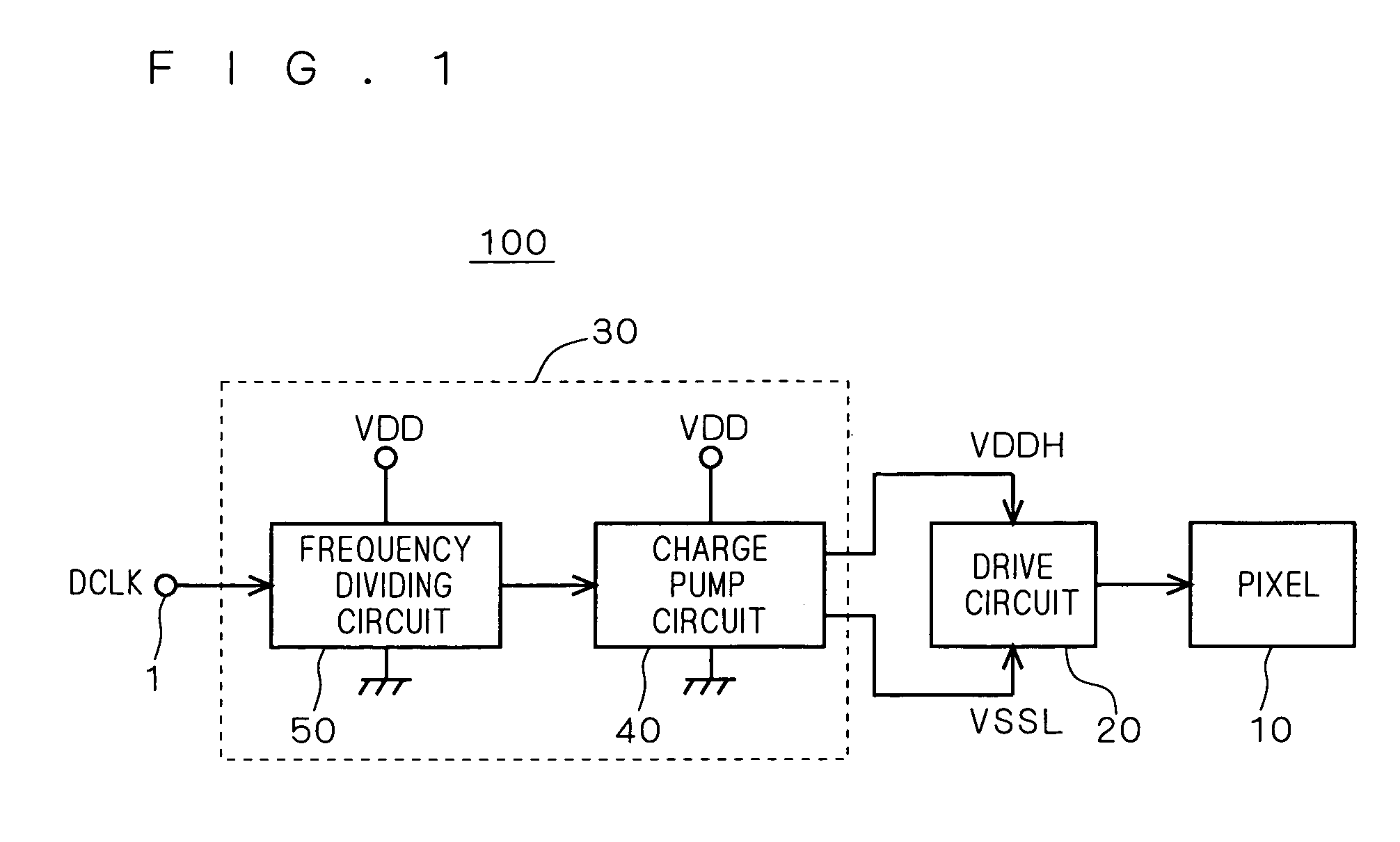
[0039]FIG. 1 is a block diagram illustrating the structure of a display device 100 according to a first preferred embodiment of the present invention.

[0040]A pixel 10 is connected to the output of a drive circuit 20. The drive circuit 20 is supplied with the voltages VDDH and VSSL from a power supply circuit 30. A dot clock signal (input signal: hereafter sometimes referred to simply as a “signal DCLK”) is input to the power supply circuit 30 from a terminal 1. The signal DCLK is at a voltage VDD on its H level and at a ground voltage (0 V, for example) on its L level.

[0041]The power supply circuit 30 produces the voltage VDDH higher than the voltage VDD and the voltage VSSL lower than the ground voltage VSS based on the signal DCLK, and outputs those voltages to the drive circuit 20. The drive circuit 20 receives VDDH and VSSL from the power supply circuit 30 to produce and output various kinds of signals for driving the pixel 10.

[0042]30>

[0043]The power supply circuit 30 inc...

second preferred embodiment

70>

[0137]FIG. 9 is a circuit diagram illustrating the structure of the charge pump circuit 70 according to a second preferred embodiment of the present invention. The corresponding parts to those in the first preferred embodiment are referred to by the same reference numerals to omit redundant descriptions.

[0138]A node N7 corresponds to the signal p1 shown in FIG. 4 in voltage level, and a node N8 to the signal P3 in voltage level. The signal P2 is supplied by the dot clock signal DCLK.

[0139]In the charge pump circuit 70 shown in FIG. 9, an inverter 73 inverts the signal DCLK to produce the inversion signal DCLK for producing the signals p1 and P3.

[0140]In FIG. 9, transistors Q9, Q12 and Q13 are N-type TFTs, and transistors Q10, Q11 and Q14 are P-type TFTs.

[0141]The transistor Q10 (second transistor) has a drain (other side terminal) connected to the output terminal 42 and one end of the output capacitance COUT (second capacitance element). The other end of the output capacitance CO...

third preferred embodiment

50>

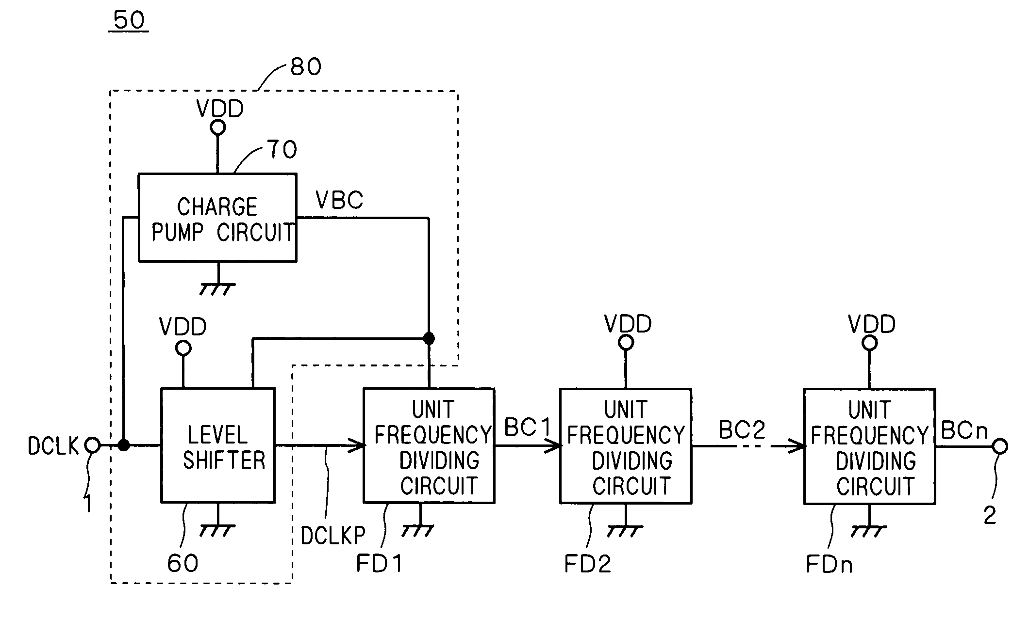
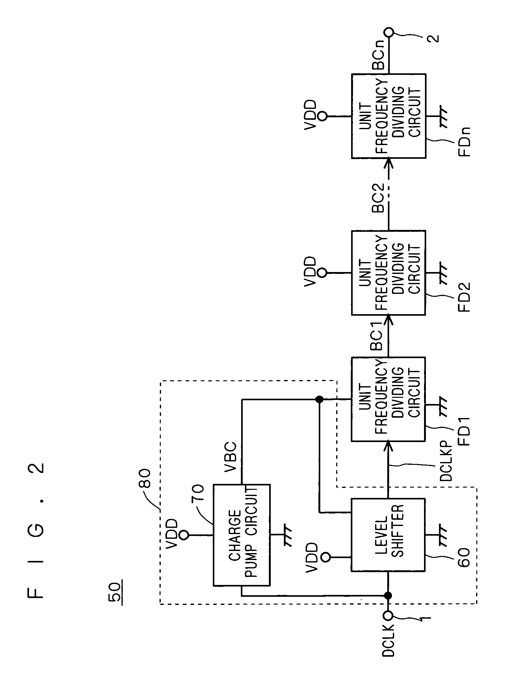
[0159]FIG. 11 is a block diagram illustrating the structure the frequency dividing circuit 50 according to a third preferred embodiment of the present invention. The corresponding parts to those in the first preferred embodiment are referred to by the same reference numerals to omit redundant descriptions.

[0160]The frequency dividing circuit 50 according to this preferred embodiment is equivalent to the frequency dividing circuit 50 according to the first preferred embodiment (see FIG. 2) that further includes a unit frequency dividing circuit FD1P (second unit frequency dividing circuit) and a level shifter 60P (second level shifter). The unit frequency dividing circuit FD1P and the level shifter 60P are structured in a similar fashion as the unit frequency dividing circuit FD1 (first unit frequency dividing circuit) and the level shifter 60, respectively.

[0161]The input of the unit frequency dividing circuit FD2 is connected to the output of an OR circuit 51. The OR circuit 51 ...


PUM


Abstract

A level shifter and a charge pump circuit are added, among cascade-connected unit frequency dividing circuits forming a frequency dividing circuit, to the unit frequency dividing circuit in the first stage. The charge pump circuit boosts an input voltage based on a dot clock signal, and supplies the booster voltage to the unit frequency dividing circuit in the first stage. The unit frequency dividing circuit in the first stage, which is driven by the booster voltage, attains an improved current driving capability. The improved current driving capability of the unit frequency dividing circuit in the first stage to which the dot clock signal of high frequency is input leads to a widened operating margin of the frequency dividing circuit.

Description

BACKGROUND OF THE INVENTION[0001]1. Field of the Invention[0002]The present invention relates to operating margin improvements of a frequency dividing circuit, a power supply circuit and a display device.[0003]2. Description of the Background Art[0004]A flat display device includes a power supply circuit and a drive circuit as well as a display element (pixel) made of liquid crystal, organic EL, or the like. The power supply circuit and drive circuit are formed by using thin film transistors (TFTs) that are formed on a substrate simultaneously with the display element.[0005]The power supply circuit includes a frequency dividing circuit and a charge pump circuit, and is supplied with a voltage VDD from an external system and a voltage VSS (GND). The frequency dividing circuit lowers the frequency of a high-frequency clock signal input thereto, and outputs a low-frequency clock signal to the charge pump circuit. The reason for lowering the frequency of the clock signal is to minimize ...

Claims


Application Information

Patent Timeline
Patent Type & Authority Patents(United States)
IPC IPC(8): H03K21/00
CPCH02M3/07H03B19/14G09G3/3696G09G2330/028H03K21/00G09G3/20
Inventor TOBITA, YOUICHIMORI, SEIICHIROUMURAI, HIROYUKI
Owner TRIVALE TECH
Why Eureka
Try Eureka