Power-on reset circuit/method for initializing an integrated circuit

a power-on reset and integrated circuit technology, applied in pulse generators, instruments, pulse techniques, etc., can solve the problems of short reset period to initialize internal circuits, internal circuits not normally initialized, and the level of power-on resetting signals will not chang

Inactive Publication Date: 2004-11-30
SOCIONEXT INC
View PDF11 Cites 9 Cited by
  • Summary
  • Abstract
  • Description
  • Claims
  • Application Information

AI Technical Summary

Problems solved by technology

As a result, for example, where the inactivation timing of the power-on reset signal shifts to the advanced side, the resetting period to initialize the internal circuits is shortened, and there is a fear that the internal circuits are not normally initialized.
Where the inactivation timing of the power-on reset signal shifts to the delayed side, there is a fear that the logic level of the power-on resetting signal will not change.

Method used


Image

  • Power-on reset circuit/method for initializing an integrated circuit
  • Power-on reset circuit/method for initializing an integrated circuit
  • Power-on reset circuit/method for initializing an integrated circuit

Examples


first embodiment

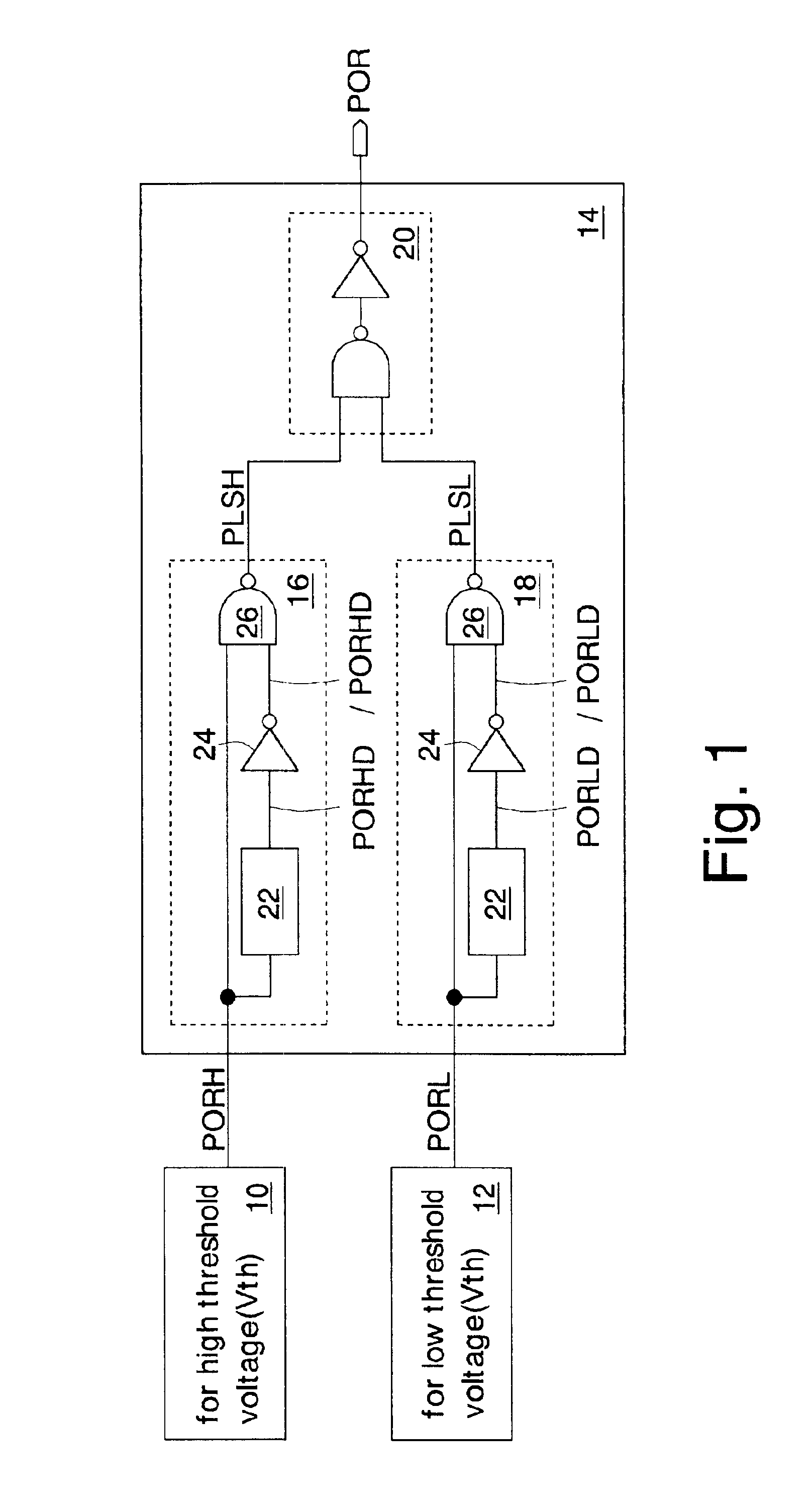
FIG. 1 shows a power-on resetting circuit according to a semiconductor integrated circuit of the invention.

The semiconductor integrated circuit is formed as a cell-based IC or a system LSI, which has an SRAM core on a silicon substrate using a CMOS process.

The power-on resetting circuit has sub reset signal generators 10 and 12, and a main reset signal generator 14. The main reset signal generator 14 has pulse generators 16 and 18 respectively corresponding to the sub reset signal generators 10 and 12 and a composite circuit 20 that receives outputs of the pulse generators 16 and 18.

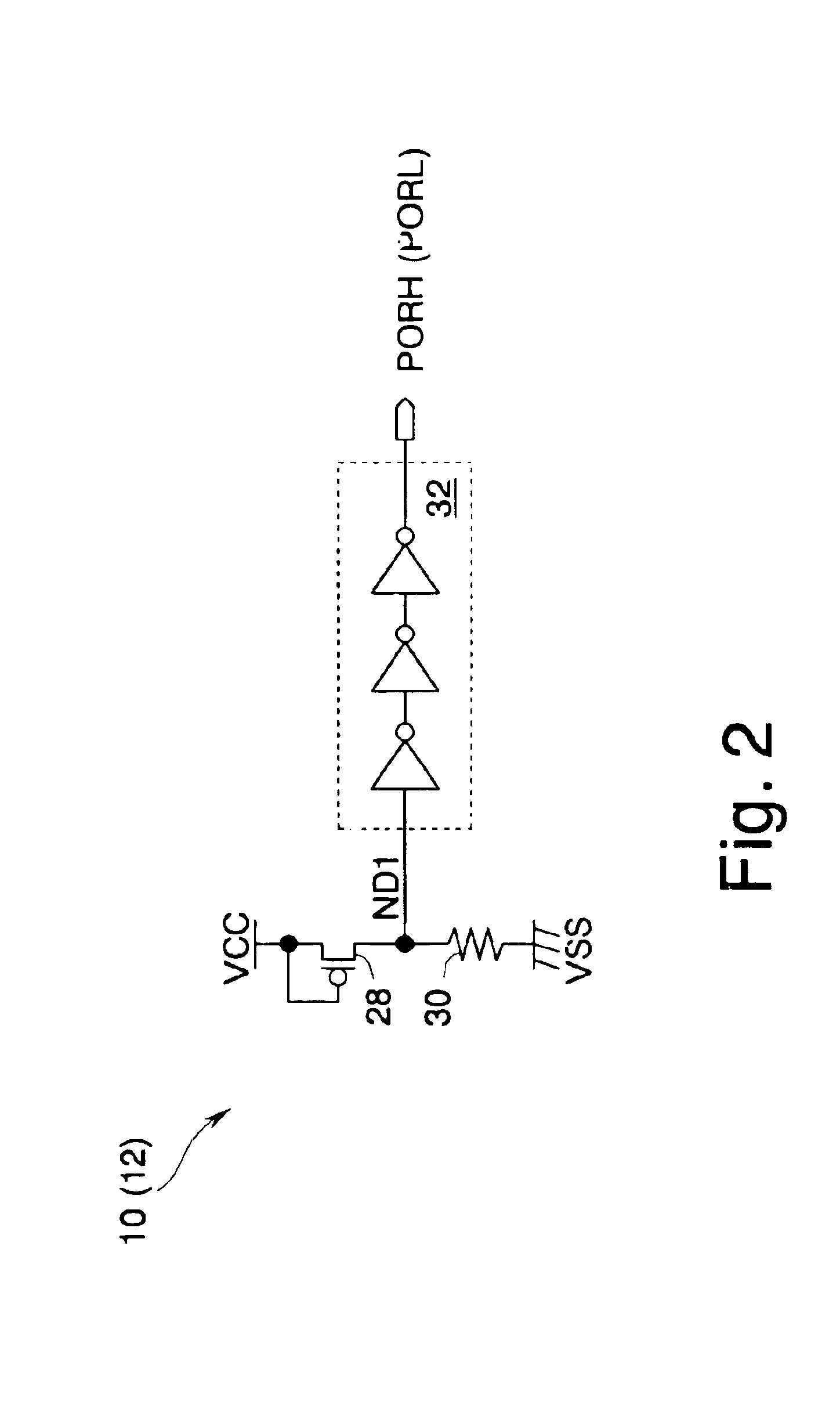
The sub reset signal generators 10 and 12 respectively generate power-on reset signals POREL and PORL. The power-on reset signal PORH is generated at an optimal timing when the threshold voltage of a transistor is high, and the power-on reset signal PORL is generated at an optimal timing when the threshold voltage of the transistor is low.

The pulse generators 16 and 18 are provided with a delay circuit 2...

second embodiment

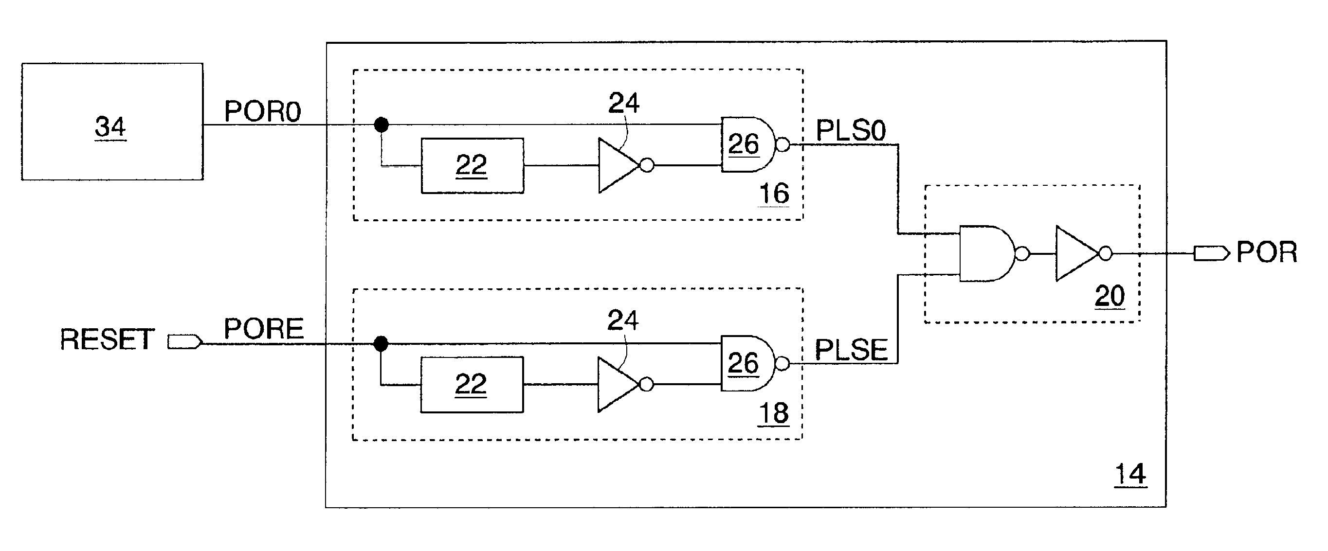
The function of a power-on resetting circuit is included in an SRAM macro. And, where an SRAM is included in a device designed by a user, the SRAM macro is used in a design tool, and the SRAM and power-on resetting circuit are laid out on the semiconductor integrated circuit.

The power-on resetting circuit is provided with one sub reset signal generator 34 and a main reset signal generator 14. The main reset signal generator 14 is the same as that of the first embodiment. The sub reset signal generator 34 generates a power-on reset signal POR0 at an optimal timing where the threshold voltage of the transistor is typical. The pulse generator 16 generates a pulse PLS0 upon receiving the power-on reset signal POR0. The pulse generator 18 generates a pulse PLSE upon receiving a power-on reset signal PORE from the periphery of the power-on resetting circuit via a reset terminal RESET. And the composite circuit 20 synthesizes pulses PLS0 and PLSE to generate a power-on reset signal POR.

In...


PUM


Abstract

The semiconductor integrated circuit is provided with a plurality of sub reset signal generators and a main reset signal generator. The sub reset signal generators respectively generate sub power-on reset signals whose timings differ from each other. The main reset signal generator generates a main power-on reset signal according to at least one from any of the sub power-on reset signals. Therefore, even where the characteristics of elements constituting the semiconductors integrated circuit change due to changes in the manufacturing conditions of the semiconductor integrated circuit, one of the sub power-on reset signals is generated at a normal timing. As a result, the main reset signal generator is able to generate a main power-on reset signal by using a normal sub power-on reset signal. That is, it is possible to constitute a power-on resetting circuit having a wide operation margin, wherein the internal circuits can be initialized without fault.

Description

1. Field of the InventionThe present invention relates to a semiconductor integrated circuit having a power-on resetting circuit and a method for initializing the semiconductor integrated circuit.2. Description of the Related ArtGenerally, a semiconductor integrated circuit has a power-on resetting circuit that generates a power-on reset signal. Malfunction of the semiconductor integrated circuit can be prevented by generating a power-on reset signal when the power supply is switched on and initializing the internal circuits. This type of a power-on resetting circuit detects, by utilizing the threshold voltage of a transistor, when the power supply voltage rises to a predetermined value, and varies (inactivates) the logic level of the power-on reset signal. The internal circuits are initialized in an activating period until the level of the power-on reset signal varies, and commences normal operation after the power-on reset signal is inactivated.Recently, the transistor structure o...

Claims


Application Information

Patent Timeline
Patent Type & Authority Patents(United States)
IPC IPC(8): H03K17/22H03K5/153G06F1/24G11C7/00H01L21/822H01L27/04
CPCH03K17/22H03K5/153G11C7/00
Inventor AKIYOSHI, HIDEO
Owner SOCIONEXT INC
Why Eureka
Try Eureka