Storage element and memory

a technology of storage elements and elements, applied in the field of storage elements and memory, can solve the problems of worsening the efficiency of spin injection, and achieve the effects of reducing the current needed for recording information, ensuring the stability of the current, and excellent characteristics of holding information

Active Publication Date: 2014-01-02
SONY CORP
View PDF1 Cites 7 Cited by
  • Summary
  • Abstract
  • Description
  • Claims
  • Application Information

AI Technical Summary

Benefits of technology

[0041]As a result, the current necessary for reversal of magnetization of the storage layer would be increased, and the spin injection efficiency would be worsened.
[0057]Furthermore, since current necessary for recording information can be reduced, operation range for recording information by passing a current can be enlarged, thereby securing widely the operation margin.

Problems solved by technology

As a result, the current necessary for reversal of magnetization of the storage layer would be increased, and the spin injection efficiency would be worsened.

Method used


Image

  • Storage element and memory
  • Storage element and memory
  • Storage element and memory

Examples


experiment 1

Examples

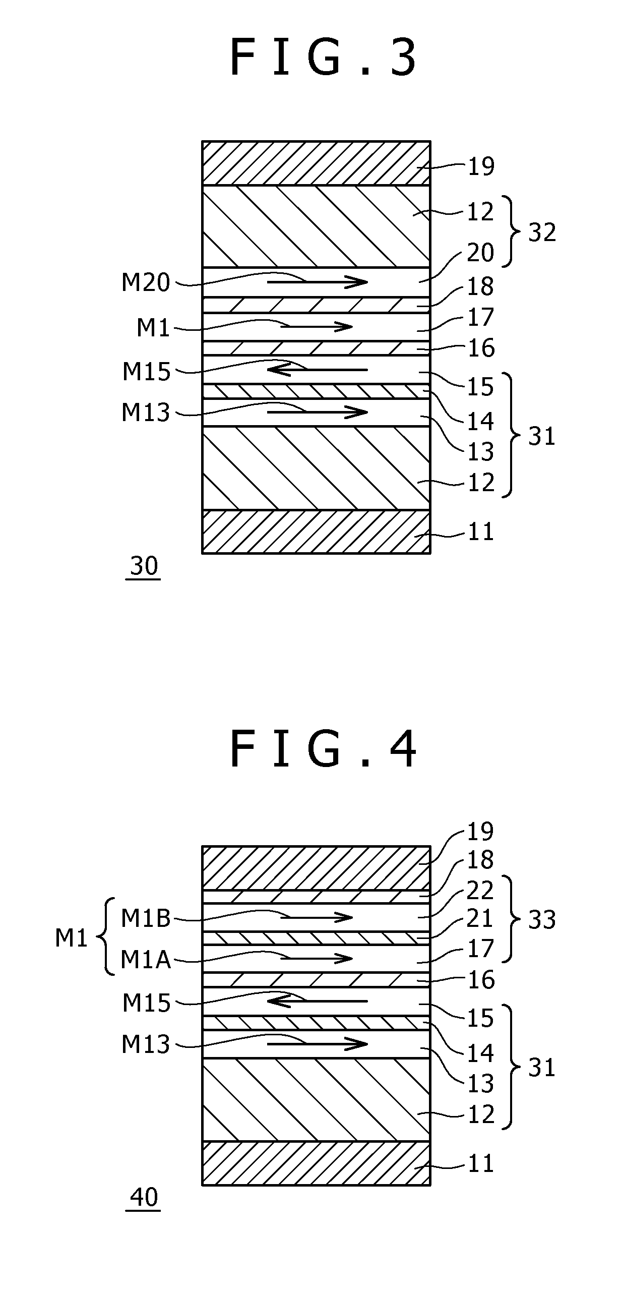
[0296]A 2 μm-thick thermal oxide film was formed on a 0.575 mm-thick silicon substrate, and a storage element 40 configured as shown in FIG. 4 was formed thereon.

[0297]Specifically, in the storage element 40 configured as shown in FIG. 4, the material and film thickness of each layer were selected as follows. The under layer 11 was composed of a 3 nm-thick Ta film, the antiferromagnetic layer 12 was composed of a 30 nm-thick PtMn film, the ferromagnetic layer 13 for constituting the pinned magnetization layer 31 was composed of a 2.2 nm-thick CoFe film, the ferromagnetic layer 15 was composed of a 2 nm-thick CoFeB film, the non-magnetic layer 14 for constituting the pinned magnetization layer 31 of the laminate ferri structure was composed of a 0.8 nm-thick Ru film, the tunnel insulation layer 16 was composed of a 0.8 nm-thick MgO film, the ferromagnetic layers 17 and 22 for constituting the storage layer 33 were each composed of a 1 nm-thick CoFeB film, the non-magnetic lay...

experiment 2

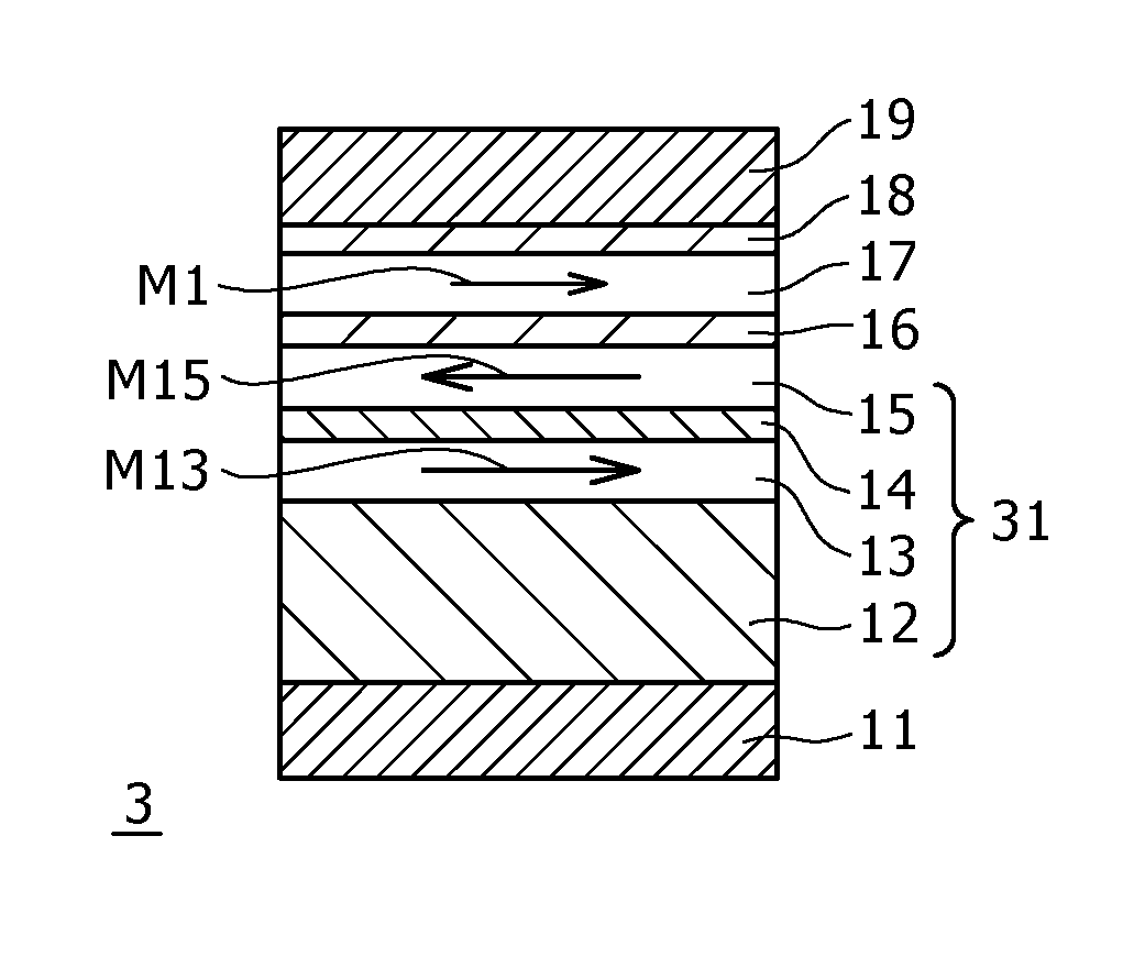
[0341]A 300 nm-thick thermal oxide film was formed on a 0.725 mm-thick silicon substrate, and a storage element 3 configured as shown in FIG. 2 was formed thereon. Besides, in forming the spin barrier layer 18 of the storage element 3, the high-resistance layer 41 and the non-magnetic metallic layer 42 were laminated, as shown in FIG. 5.

[0342]Specifically, in the storage element 3 configured as shown in FIG. 2, the material and film thickness of each layer were selected as follows. The under layer 11 was composed of a 3 nm-thick Ta film, the antiferromagnetic layer 12 was composed of a 20 nm-thick PtMn film, the ferromagnetic layer 13 for constituting the pinned magnetization layer 31 was composed of a 2 nm-thick CoFe film, the ferromagnetic layer 15 was composed of a 2.5 nm-thick CoFeB film, the non-magnetic layer 14 for constituting the pinned magnetization layer 31 of the laminate ferri structure was composed of a 0.8 nm-thick Ru film, the tunnel insulation layer 16 was composed ...

experiment 3

[0355]Samples of storage element 3 were prepared in the same manner as the samples of storage element 3 in Experiment 2, except that the non-magnetic metallic layer 42 to be the spin barrier layer 18 in the storage element 3 configured as shown in FIG. 2 was composed of a 5 nm-thick Ta film.

[0356]Then, samples differing in the thickness of the magnesium oxide film of the high-resistance layer 41 to be the spin barrier layer 18 were prepared. Specifically, samples of storage element 3 were prepared while setting the thickness of the magnesium oxide film after sputtering to be 0.5 nm, 0.7 nm, 0.9 nm, 1.1 nm, and 1.3 nm, respectively.


PUM


Abstract

A storage element including a storage layer configured to hold information by use of a magnetization state of a magnetic material, with a pinned magnetization layer being provided on one side of the storage layer, with a tunnel insulation layer, and with the direction of magnetization of the storage layer being changed through injection of spin polarized electrons by passing a current in the lamination direction, so as to record information in the storage layer, wherein a spin barrier layer configured to restrain diffusion of the spin polarized electrons is provided on the side, opposite to the pinned magnetization layer, of the storage layer; and the spin barrier layer includes at least one material selected from the group composing of oxides, nitrides, and fluorides.

Description

CROSS REFERENCES TO RELATED APPLICATIONS[0001]This application is a continuation of U.S. patent application Ser. No. 11 / 564,595 filed Nov. 29, 2006, the entirety of which is incorporated herein by reference to the extent permitted by law. The present invention contains subject matter related to Japanese Patent Application JP 2005-348112 filed with the Japanese Patent Office on Dec. 1, 2005, the entire contents of which being incorporated herein by reference.BACKGROUND OF THE INVENTION[0002]1. Field of the Invention[0003]The present invention relates to a storage element including a storage layer for storing a magnetization state of a ferromagnetic layer as information, and a pinned magnetization layer with its magnetization direction fixed, wherein the direction of magnetization of the storage layer is changed through injection of spin polarized electrons therein by passing a current in a direction perpendicular to the film plane, and to a memory including the storage elements. The ...

Claims


Application Information

Patent Timeline
Patent Type & Authority Applications(United States)
IPC IPC(8): H01L43/10
CPCH01L43/10B82Y10/00B82Y25/00H10B61/22H10N50/10G11C11/15G11C11/02H10N50/85H10N50/80
Inventor HIGO, YUTAKAHOSOMI, MASANORIBESSHO, KAZUHIROYAMAMOTO, TETSUYAOHMORI, HIROYUKIYAMANE, KAZUTAKAOISHI, YUKIKANO, HIROSHI
Owner SONY CORP
Why Eureka
Try Eureka