Planar electroluminescent devices and uses thereof

a technology of electroluminescent devices and planar beams, applied in the field of electroluminescence, can solve the problems of difficult realization of potential applications, doubt of significance, and low attention on the subject of phenomenon, and achieve the effect of less luminance and reduced luminan

Active Publication Date: 2018-03-29
PEKING UNIV SHENZHEN GRADUATE SCHOOL
View PDF3 Cites 27 Cited by
  • Summary
  • Abstract
  • Description
  • Claims
  • Application Information

AI Technical Summary

Benefits of technology

[0020]In one embodiment, the above device further comprises hole injection layer (HIL), hole transport layer (HTL), electron injection layer (EIL) and electrode transport layer (ETL). As used herein, HIL refers to an interface connection layer between the anode and the HTL, which would have good adhesion to the anode and would serve to smooth the anode surface. It can improve the film forming property of the subsequent organic layer and facilitate efficient hole injection.
[0043]In one embodiment, the modulating polarization layer would include fluorescent or phosphorescent material. It should be noted that addition of fluorescent or phosphorescent material is intended to improve the luminance and change the light color. In other words, after adding a modulating layer, the device can emit light; if one add some different fluorescence or phosphorescent materials in the modulating polarization layer, the device can emit light with different colors.

Problems solved by technology

But, in the following 10 years, this phenomenon did not attract much attention.
Its significance was doubted and it was hard to realize its potential applications.
Nevertheless, after another 10 years, limitations on the brightness, life-time and light color of alternating current electroluminescent devices (referred to as ACEL) became evident and people's enthusiasm about EL devices began to subside.
Moreover, these EL devices having vertical structure with top and bottom electrodes present serious problems like: (1) such structure can only be used for display lighting and cannot meet more diverse needs and uses; (2) since both top and bottom electrodes are required, the production process is more complex and production cost is higher; (3) the structure requires one transparent electrode.
If the bottom electrode is transparent, it also requires a transparent substrate, thereby restricting the choice of substrate material.

Method used


Image

  • Planar electroluminescent devices and uses thereof
  • Planar electroluminescent devices and uses thereof
  • Planar electroluminescent devices and uses thereof

Examples


example 1

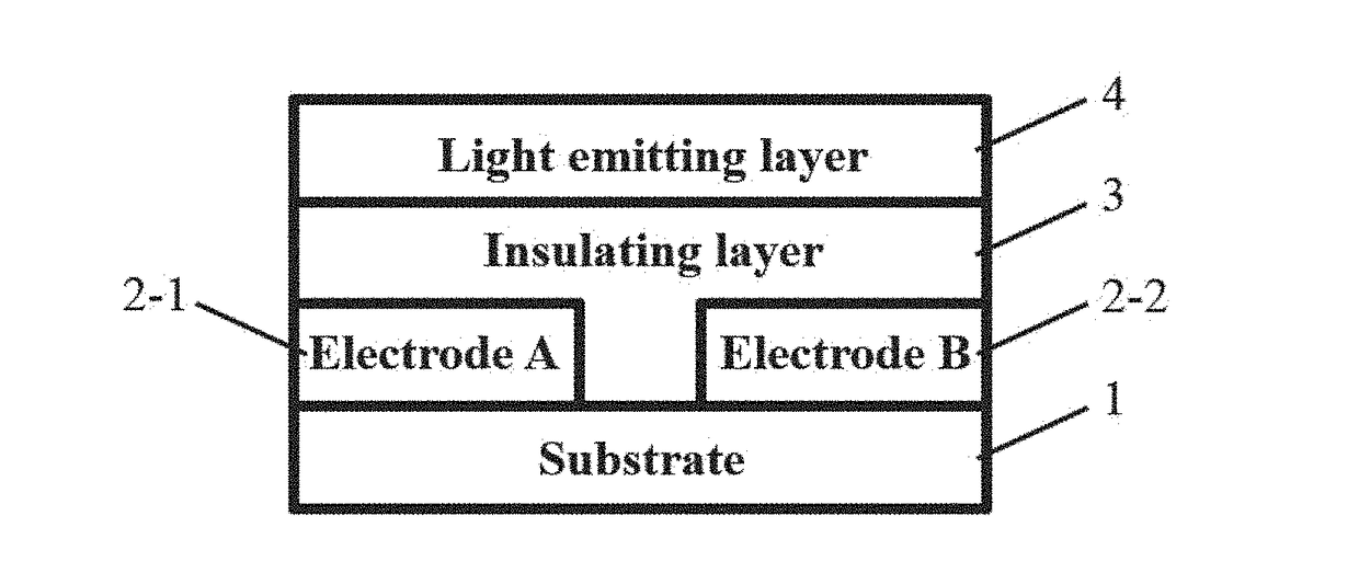
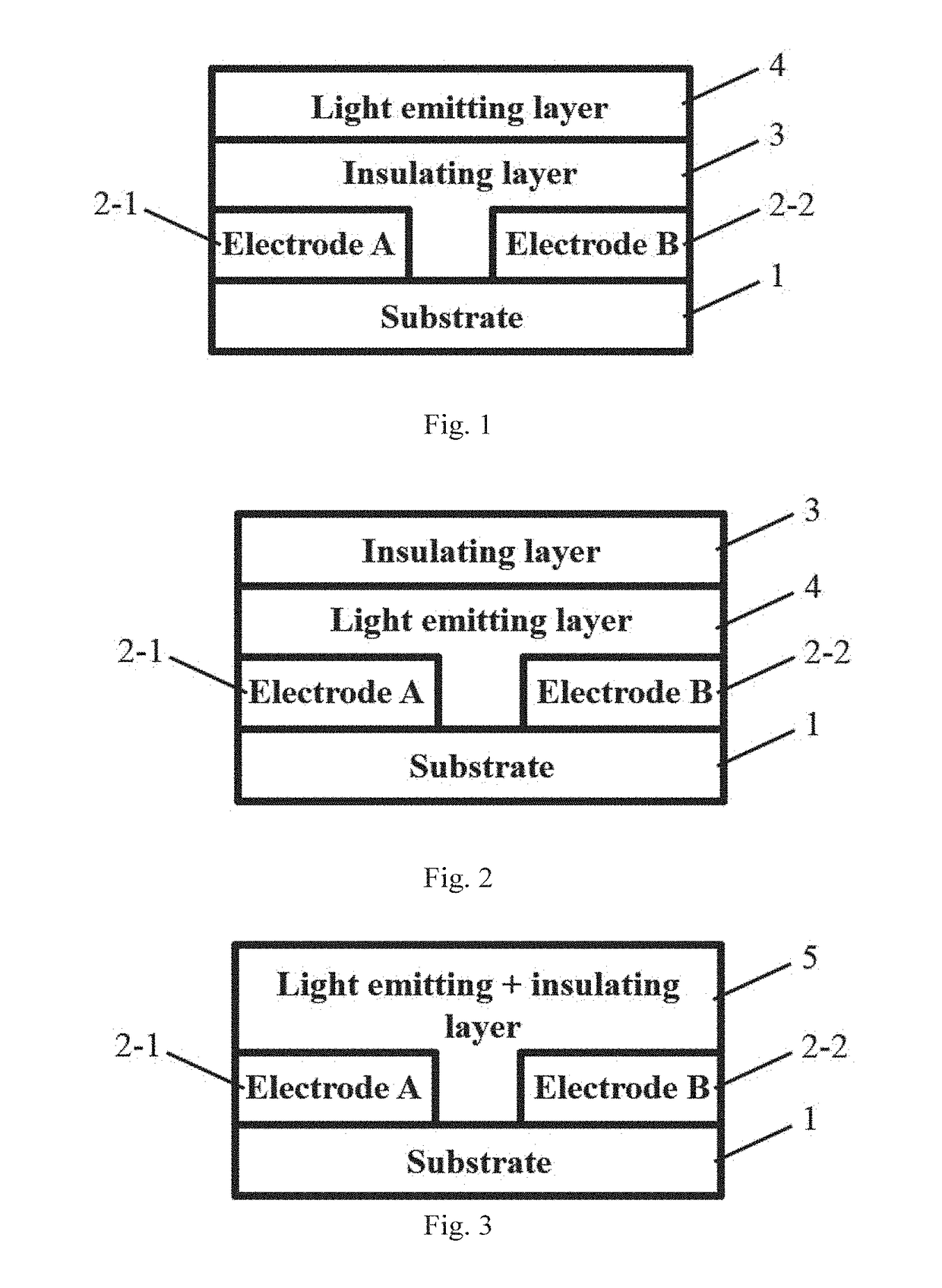
[0138]In this example, PET plastic is used as a substrate, and the method of fabrication is screen printing. The structure of the planar electroluminescent device is shown in FIG. 1, comprising a substrate layer 1, an electrode layer, an insulating layer 3 and a light emitting layer 4. In one embodiment, the electrode layer includes electrode A 2-1 and electrode B 2-2. The electrodes are printed on the surface of the substrate 1 with gap in between, and form an electrode layer. Adjacent electrodes A 2-1 and the electrode B 2-2 are not in contact with each other. The electrode layer is sandwiched between the insulating layer 3 and the substrate layer 1. The light emitting layer 4 is fabricated on the surface of the insulating layer 3.

[0139]In one embodiment, in order to prevent the PET plastic substrate from shrinking in subsequent drying process, and prevent the electrodes from being bonded together to cause a short circuit, the PET plastic was dried in an oven at 100° C. for 30 min...

example 2

[0151]This example shows the relationships between different frequency, voltage and luminance when the planar electroluminescent device was configured as an electroluminescent writing board. Water is used as writing fluid.

Varying Input Voltage at Constant Frequency

[0152]Deionized water was dropped onto the planar electroluminescent device, and tested on a 3 cm×3 cm glass sheet area. EL cold light equipment was used to measure the luminance. The device was tested at constant frequency of 500 Hz, 1000 Hz, 1500 Hz, or 3000 Hz, whereas the input voltage was changed from 0 to 180 V. For example, at 500 Hz, the luminance was measured at 0-180 V; at 1000 Hz, the luminance was measured at 0-180 V; at 1500 Hz, the luminance was measured at 0-180 V; at 3000 Hz, the luminance was measured at 0-180 V.

[0153]As shown in FIG. 17, it can be seen that as the voltage is increased, the luminance is also increased. Also, as the frequency is increased, so is the luminance. And the luminance will eventua...

example 3

[0156]This example shows the effects of the size of the gap area between adjacent electrodes on luminance. Adjacent electrodes in the EL device of example 1 have a gap area between them at 0.5 mm wide. In this example, the space between electrodes A and electrodes B is varied to 0.4 mm, 1.0 mm, 1.75 mm, or 3.2 mm. Other parts of the EL device are arranged as in those in Example 1.

[0157]Deionized water was dropped onto the planar electroluminescent device, and tested on a 3 cm×3 cm glass sheet area. EL cold light equipment was used to measure the luminance. Luminance was measured at 1000 Hz at 60 V, 100 V, 120 V, or 140 V. As shown in FIG. 19, the luminance decreases when the gap width of the electrodes increases. And at higher voltage, the change in the amplitude of the luminance is also greater.


PUM

PropertyMeasurementUnit
conductivityaaaaaaaaaa
internal quantum efficiencyaaaaaaaaaa
sizeaaaaaaaaaa

Abstract

The present invention provides a planar electroluminescence (EL) device comprising a substrate layer, an electrode layer, a light emitting layer, and a modulating layer, wherein the electrode layer comprises a plurality of electrodes arranged on a same level over the substrate layer, and there is no contact between adjacent electrodes. In one embodiment, the device further comprises a hole injection layer (HIL), a hole transport layer (HTL), an electron injection layer (EIL) and an electrode transport layer (ETL). In one embodiment, the light emitting layer comprises organic light emitting polymers or organic light emitting molecules. The device of the present invention would emit light when liquid, polar component, or conductive solution is written directly on the light emitting layer. In one embodiment, the device can emit light for prolonged period when the light emitting layer is coated or deposited with conductive material.

Description

[0001]This application claims the benefit of priority of International application No. PCT / US2016 / 037825, filed Jun. 16, 2016, which claims the priority of Chinese application No. 201510345516.4, filed Jun. 19, 2015. This application also claims the benefit of priority of Chinese application No. 201710168774.9, filed Mar. 21, 2017. The entire content and disclosure of the preceding applications are incorporated by reference into this application.FIELD OF THE INVENTION[0002]This application is related generally to the area of electroluminescence. In one embodiment, there is provided electroluminescent devices and uses thereof.BACKGROUND OF THE INVENTION[0003]The electric field-induced luminescence is also known as Electroluminescence (EL). In 1936, a French scientist G. Destriau discovered this phenomenon for the first time, so it is an 80 years old technology. Destriau found that a powdered fluorescent material when immersed in liquid dielectric material can generate continuous brig...

Claims


Application Information

Patent Timeline
Patent Type & Authority Applications(United States)
IPC IPC(8): H01L51/52H01L51/00H01L51/50C09K11/06B43L1/00
CPCH01L51/5206H01L51/0096H01L51/5221H01L51/5088H01L51/5056H01L51/5092H01L51/5072H01L51/5253H01L51/5262C09K11/06B43L1/006H01L51/0078H01L51/0037H01L51/0035H01L51/0094H01L2251/303H01L2251/301H01L51/0059H01L51/0072H01L51/0061H01L51/006H01L51/0058H01L51/0081H01L51/0092H01L51/0077H01L51/007H01L2051/0063H01L2251/558H01L51/004C09K2211/186C09K2211/1022C09K2211/1029H10K50/805Y02E10/549H10K50/81H10K50/15H10K50/16H10K50/17H10K50/82H10K50/85H10K50/171H10K50/844H10K77/10H10K85/30H10K85/40H10K85/111H10K85/141H10K85/311H10K85/324H10K85/381H10K85/626H10K85/631H10K85/633H10K85/636H10K85/1135H10K85/6565H10K85/6572H10K2102/00H10K2102/351
Inventor MENG, HONGHU, DANXU, XIURUYAN, LIJIAHUANG, WEI
Owner PEKING UNIV SHENZHEN GRADUATE SCHOOL
Why Eureka
Try Eureka