

Electrode, method for forming an electrode, thin-film transistor, electronic circuit, organic electroluminescent element, display, and electronic equipment
a thin-film transistor and electrode technology, applied in the field of electrodes, can solve the problems of low efficiency in injecting carriers (holes), lowering transistor properties, and reducing the efficiency of electrode insertion, so as to enhance the property (switching property) of the thin-film transistor, high reliability and high reliability
- Summary
- Abstract
- Description
- Claims
- Application Information
AI Technical Summary
Benefits of technology
Problems solved by technology
Method used
Image

Examples
first exemplary embodiment
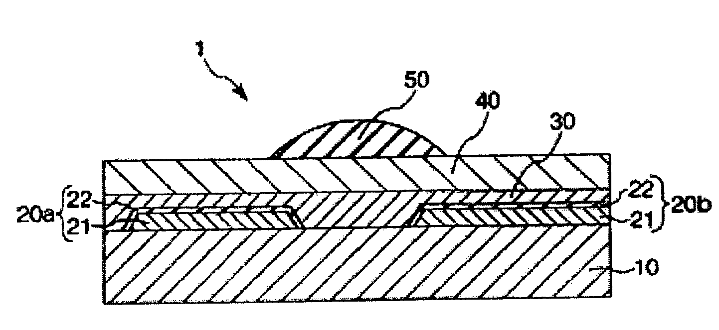
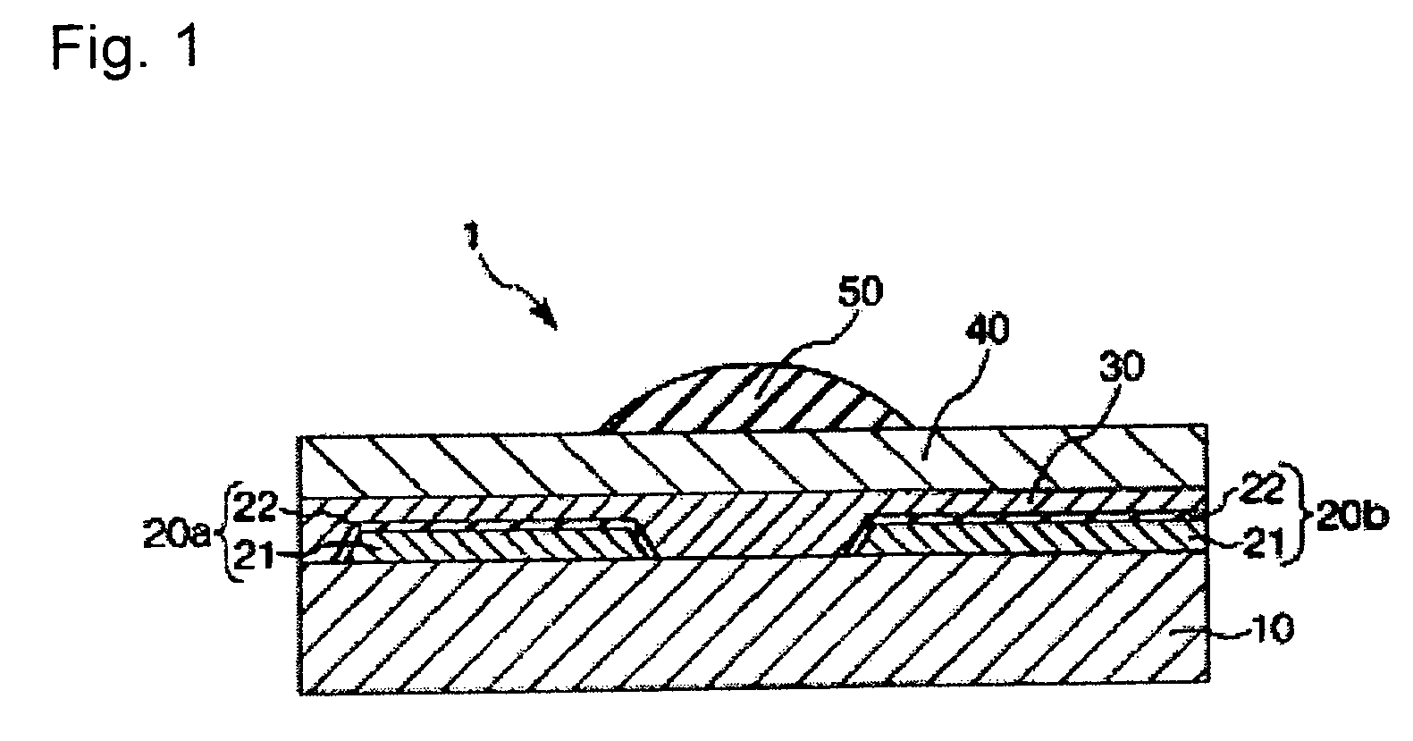
[0039]A thin-film transistor according to a first exemplary embodiment of the present invention will now be described.
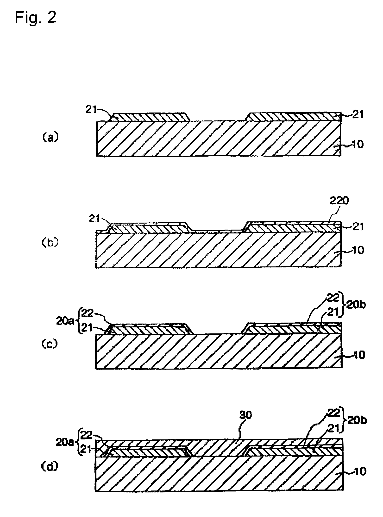
[0040]FIG. 1 is a schematic showing a thin-film transistor according to the first exemplary embodiment of the present invention. FIGS. 2(a)-2(d) and 3(e) and 3(f) are schematics illustrating a method to manufacture the thin-film transistor shown in FIG. 1.
[0041]A thin-film transistor 1 shown in FIG. 1 is a top-gate thin-film transistor. The thin-film transistor 1 includes a source electrode 20a and a drain electrode 20b that are placed separately from each other. The thin-film transistor 1 also includes an organic semiconductor layer 30 that is laid out between the source electrode 20a and the drain electrode 20b, and a gate insulating layer 40 that is provided between the organic semiconductor layer 30 and a gate electrode 50. This structure is mounted on a substrate 10.
[0042]Each element will now be described in greater detail. The substrate 10 supports each layer ...
second exemplary embodiment
[0086]A thin-film transistor according to a second exemplary embodiment of the present invention will now be described.
[0087]FIG. 4 is a schematic showing the thin-film transistor according to the second exemplary embodiment of the present invention. FIGS. 5(a)-5(c) are schematics illustrating a method to manufacture the thin-film transistor shown in FIG. 4. The thin-film transistor according to the second exemplary embodiment will be described below, mainly in terms of differences from the thin-film transistor according to the first exemplary embodiment. The description of what the two have in common will be omitted.
[0088]The thin-film transistor 1 of the second exemplary embodiment has the source electrode 20a and the drain electrode 20b of different structures from those included in the thin-film transistor 1 of the first exemplary embodiment, which is the only difference between the two. Here, each of the source electrode 20a and the drain electrode 20b has a single-layer struct...
third exemplary embodiment
[0101]A thin-film transistor according to a third exemplary embodiment of the present invention will now be described.
[0102]FIG. 6 is a schematic showing the thin-film transistor of the third exemplary embodiment of the present invention. The thin-film transistor according to the third exemplary embodiment will be described below mainly in terms of differences from the thin-film transistor according to the first exemplary embodiment. The description of what the two have in common will be omitted.
[0103]The thin-film transistor 1 of the third exemplary embodiment has an overall structure that is different from that of the thin-film transistor 1 of the first exemplary embodiment, which is the only difference between the two. Specifically, the thin-film transistor 1 shown in FIG. 6 is a bottom-gate thin-film transistor in which the gate electrode 50 is provided, not on the side of the source electrode 20a and the drain electrode 20b, but on the substrate 10 side with the gate insulating...
PUM
 Abstract
Description
Claims
Application Information