Frequency dividing circuit, power supply circuit and display device

Active Publication Date: 2006-09-21
TRIVALE TECH
View PDF9 Cites 13 Cited by
  • Summary
  • Abstract
  • Description
  • Claims
  • Application Information

AI Technical Summary

Benefits of technology

[0014] At least the unit frequency dividing circuit in the first stage of the frequency dividing circuit is activated by using the booster voltage. This leads to an improvement in curren

Problems solved by technology

The present TFT formed by a low-temperature polysilicon process, however, is low in current driving capability, and will not follo

Method used


Image

  • Frequency dividing circuit, power supply circuit and display device
  • Frequency dividing circuit, power supply circuit and display device
  • Frequency dividing circuit, power supply circuit and display device

Examples


Embodiment Construction

[0038]

[0039]

[0040]

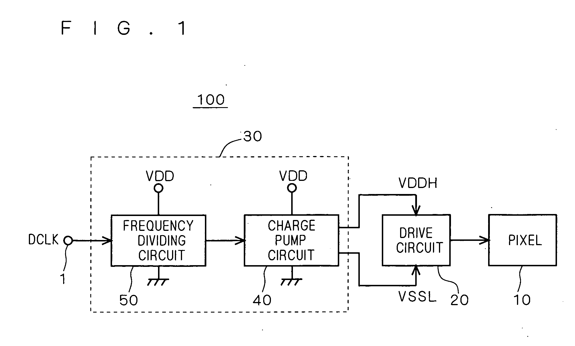
[0041]FIG. 1 is a block diagram illustrating the structure of a display device 100 according to a first preferred embodiment of the present invention.

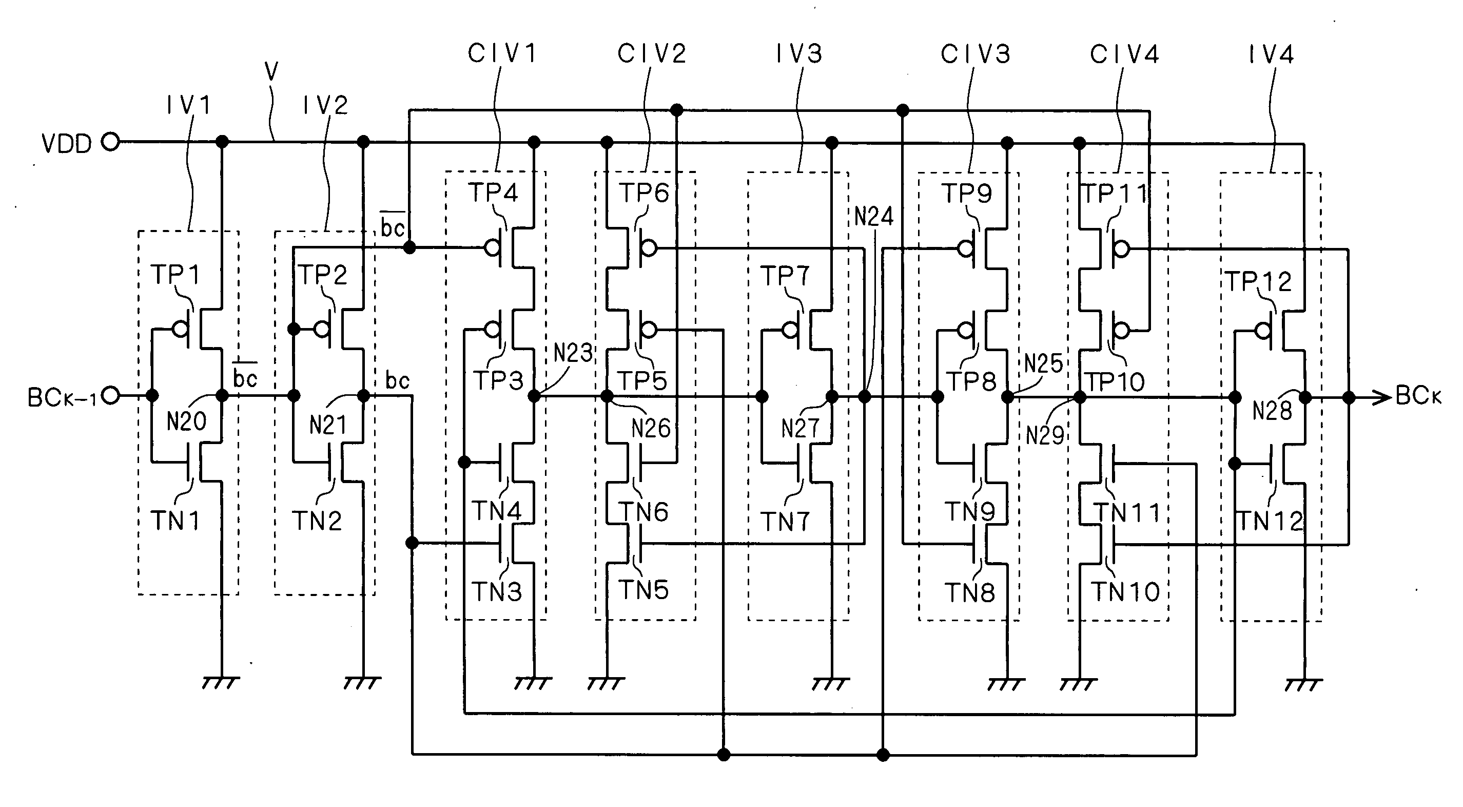
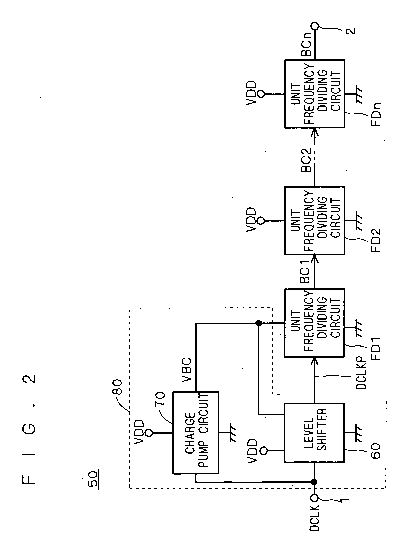
[0042] A pixel 10 is connected to the output of a drive circuit 20. The drive circuit 20 is supplied with the voltages VDDH and VSSL from a power supply circuit 30. A dot clock signal (input signal: hereafter sometimes referred to simply as a “signal DCLK”) is input to the power supply circuit 30 from a terminal 1. The signal DCLK is at a voltage VDD on its H level and at a ground voltage (0 V, for example) on its L level.

[0043] The power supply circuit 30 produces the voltage VDDH higher than the voltage VDD and the voltage VSSL lower than the ground voltage VSS based on the signal DCLK, and outputs those voltages to the drive circuit 20. The drive circuit 20 receives VDDH and VSSL from the power supply circuit 30 to produce and output various kinds of signals for driving the pixel 10.

[0044]30>

[0045] The power sup...


PUM


Abstract

A level shifter and a charge pump circuit are added, among cascade-connected unit frequency dividing circuits forming a frequency dividing circuit, to the unit frequency dividing circuit in the first stage. The charge pump circuit boosts an input voltage based on a dot clock signal, and supplies the booster voltage to the unit frequency dividing circuit in the first stage. The unit frequency dividing circuit in the first stage, which is driven by the booster voltage, attains an improved current driving capability. The improved current driving capability of the unit frequency dividing circuit in the first stage to which the dot clock signal of high frequency is input leads to a widened operating margin of the frequency dividing circuit.

Description

BACKGROUND OF THE INVENTION [0001] 1. Field of the Invention [0002] The present invention relates to operating margin improvements of a frequency dividing circuit, a power supply circuit and a display device. [0003] 2. Description of the Background Art [0004] A flat display device includes a power supply circuit and a drive circuit as well as a display element (pixel) made of liquid crystal, organic EL, or the like. The power supply circuit and drive circuit are formed by using thin film transistors (TFTs) that are formed on a substrate simultaneously with the display element. [0005] The power supply circuit includes a frequency dividing circuit and a charge pump circuit, and is supplied with a voltage VDD from an external system and a voltage VSS (GND). The frequency dividing circuit lowers the frequency of a high-frequency clock signal input thereto, and outputs a low-frequency clock signal to the charge pump circuit. The reason for lowering the frequency of the clock signal is to...

Claims


Application Information

Patent Timeline
IPC IPC(8): H03B19/00
CPCG09G3/3696G09G2330/028H02M3/07H03B19/14G09G3/20H03K21/00
Inventor TOBITA, YOUICHIMORI, SEIICHIROUMURAI, HIROYUKI
Owner TRIVALE TECH
Why Eureka
Try Eureka