Manufacturing method of three-dimensional array grid-last type Si-NWFET (Nanowire Field Effect Transistor) based on SOI (Silicon On Insulator)

A technology of three-dimensional arrays and manufacturing methods, which is applied in semiconductor/solid-state device manufacturing, nanotechnology for information processing, electrical components, etc., can solve problems such as inconvenience, unsuitability for field-effect transistor gate oxide layers, and large interface states. Achieve the effects of simplifying the process, increasing the number of nanometer lines, and increasing the current driving capability of the device

Inactive Publication Date: 2012-08-01
SHANGHAI HUALI MICROELECTRONICS CORP
View PDF3 Cites 10 Cited by
  • Summary
  • Abstract
  • Description
  • Claims
  • Application Information

AI Technical Summary

Problems solved by technology

This method can realize the vertically stacked silicon nanowire field effect transistor structure, but there is a disadvantage: when the SiGe layer is oxidized, Ge will be concentrated on the surface of the Si layer. SiGe alloy
Because GeO2 is soluble in water, it

Method used


Image

  • Manufacturing method of three-dimensional array grid-last type Si-NWFET (Nanowire Field Effect Transistor) based on SOI (Silicon On Insulator)
  • Manufacturing method of three-dimensional array grid-last type Si-NWFET (Nanowire Field Effect Transistor) based on SOI (Silicon On Insulator)
  • Manufacturing method of three-dimensional array grid-last type Si-NWFET (Nanowire Field Effect Transistor) based on SOI (Silicon On Insulator)

Examples


Embodiment Construction

[0067] In order to make the above objects, features and advantages of the present invention more comprehensible, specific implementations of the present invention will be described in detail below in conjunction with the accompanying drawings.

[0068] First, if Figure 22 As shown, in order to describe this embodiment more clearly, define the fin-shaped active region or the length direction of the subsequently formed silicon nanowire as XX' direction, XX' direction runs through the gate and source and drain regions, and is perpendicular to X-X' direction is Y-Y' direction. Combine below Figures 1 to 22 Describe in detail the method for manufacturing a bulk silicon-based three-dimensional array Si-NWFET according to an embodiment of the present invention, specifically including:

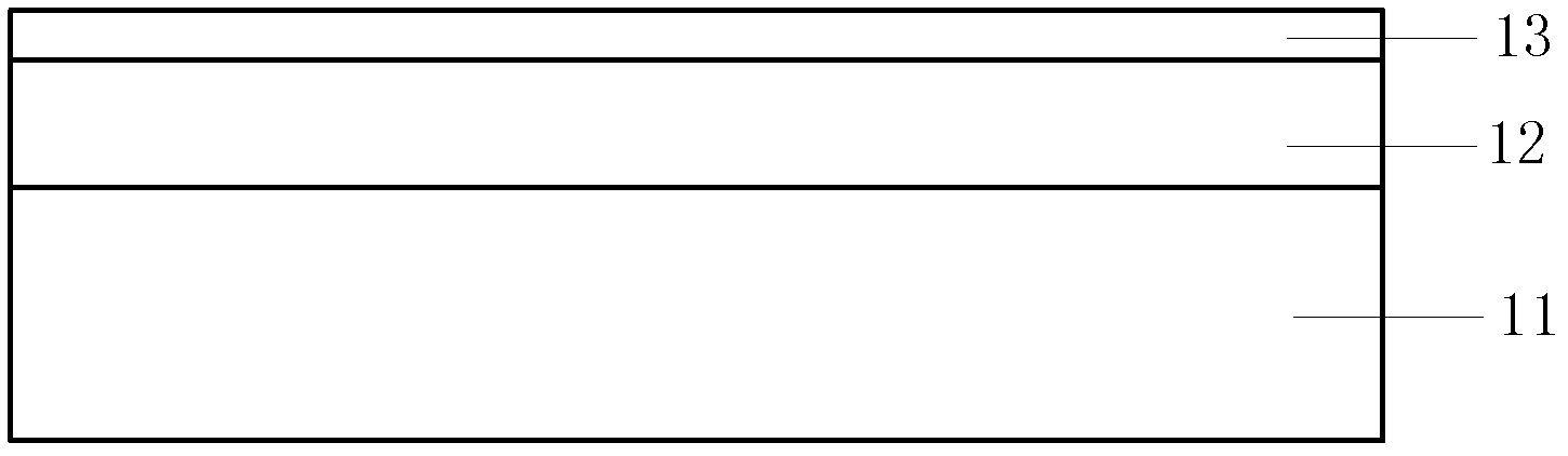
[0069] Please refer to figure 1 , provide an SOI substrate, the bottom layer of the SOI substrate is a silicon liner 11 for providing mechanical support, an insulator layer is provided on the sil...


PUM

PropertyMeasurementUnit
Diameteraaaaaaaaaa

Abstract

The invention discloses a manufacturing method of a three-dimensional array grid-last type Si-NWFET (Silicon-Nanowire Field Effect Transistor) based on an SOI (Silicon On Insulator). The manufacturing method comprises the following steps of: alternatively growing silicon layers and germanium-silicon layers on the SOI, forming a fin-shaped active region, forming silicon nanowires in the fin-shaped active region, depositing amorphous carbon in a groove as a virtual isolating layer, then carrying out a grid-last process, and finally and simultaneously carrying out deposition on a groove isolating medium and an interlayer isolating medium. The manufacturing method disclosed by the invention has the advantages that due to existence of an oxygen embedding layer in the SOI, the isolating effect between a grid and an SOI substrate is effectively improved, and the adoption of the grid-last process is beneficial to the control of the profile of the grid and the electrical property of a device; the utilization of the amorphous carbon as the virtual isolating layer is beneficial to the control of the profiles of the grid and the grid groove; and in addition, the silicon-nanowire field effect transistor (Si-NWFET) structure is designed by adopting a three-dimensional array silicon-nanowire structure, so that the number of the nanowires is increased, and the current driving capability of the device is improved.

Description

technical field [0001] The invention relates to the field of integrated circuit manufacturing, in particular to an SOI-based three-dimensional array gate-back Si-NWFET manufacturing method. Background technique [0002] It has always been the goal pursued by the development of microelectronics industry to increase the working speed and integration of chips and reduce the power consumption density of chips by reducing the size of transistors. In the past forty years, the development of microelectronics industry has been following Moore's Law. At present, the physical gate length of field effect transistors is close to 20nm, and the gate dielectric is only a few layers of oxygen atoms thick. It is difficult to improve performance by reducing the size of traditional field effect transistors, mainly because of the short Channeling and gate leakage destroy the switching performance of transistors. [0003] Nanowire Field Effect Transistor (NWFET, Nano-Wire MOSFET) is expected t...

Claims


Application Information

Patent Timeline
IPC IPC(8): H01L21/762H01L21/28H01L21/02H01L21/336
CPCB82Y40/00B82Y10/00H01L29/0673H01L29/42392H01L29/66439H01L29/775H01L29/78696
Inventor 黄晓橹刘格致
Owner SHANGHAI HUALI MICROELECTRONICS CORP
Why Eureka
Try Eureka