Semiconductor device having current change memory cell

a memory cell and semiconductor technology, applied in the direction of digital storage, electrical analogue stores, instruments, etc., can solve the problems of reducing the speed with which the sense amplifier drives the global bit line, the inability to achieve a semiconductor device capable of high-speed read operation, and the inability to achieve high-speed read operation. , to achieve the effect of maintaining the potential of the sense node, and suppressing an increase in area

Inactive Publication Date: 2013-11-19
LONGITUDE LICENSING LTD
View PDF10 Cites 10 Cited by
  • Summary
  • Abstract
  • Description
  • Claims
  • Application Information

AI Technical Summary

Benefits of technology

[0011]According to the semiconductor device of the invention, in the read operation of the current change memory cell, the first transistor functions as a charge transfer gate, which controls a charge transfer between the bit line and the sense node in response to the transfer control voltage (the first potential) applied to its gate. In order to achieve a low voltage operation in the semiconductor device, the third potential supplied to the bit line needs to be set to a low value. In contrast, the second potential supplied to the sense node needs to be set higher than the third potential to improve current driving ability of the second transistor, thereby speeding up the read operation. In the semiconductor device of the invention, the second potential is set higher than the third potential, and the predetermined potential (the potential obtained by subtracting the threshold voltage of the first transistor from the first potential) at which the first transistor is switched on (conductive) and off (non-conductive) is set within a range including the third potential and the low potential corresponding to binary data that can be stored in the memory cell, thereby achieving a high-speed read operation of the sense amplifier by controlling the charge transfer between the bit line and the sense node.
[0012]The invention can be applied to various configurations of the memory cell array, and particularly, the invention can be effectively applied to a memory cell array having the hierarchical bit line. That is, by applying the invention to the configuration in which there are provided local bit lines of a lower hierarchy and global bit lines of an upper hierarchy and global sense amplifiers that amplify signals transmitted through the global bit lines through local sense amplifiers connected to the local bit lines, it is possible to suppress an increase in area and an increase in consumption current, and to achieve the high-speed read operation.
[0014]As described above, according to the present invention, in the semiconductor device having a configuration in which data stored in the current change memory cell is read out to the bit line and amplified by the sense amplifier through the charge transfer gate, the potential of the sense node is maintained high even when the bit line voltage is lowered, and thus it is possible to perform the high-speed read operation.
[0015]Further, in the semiconductor device in which the memory cell array is hierarchized, when the signal transmitted from the local bit line to the global bit line via the local sense amplifier is amplified by the global sense amplifier, it is possible to suppress an increase in area and an increase in consumption current and to achieve the high-speed read operation.
[0016]Furthermore, the process variation and the temperature dependence of the threshold voltage of the first transistor are compensated for the first potential that is supplied to the first transistor as the charge transfer gate, it is possible to further improve the operating margin in the read operation.

Problems solved by technology

Therefore, when the gate voltage is decreased with miniaturization of the memory cells, there causes a decrease in speed with which the sense amplifier drives the global bit line.
Meanwhile, according to the technique disclosed in Patent Reference 2, when the charge is transferred between the bit line and the sense node via the charge transfer gate (Q1), potential settings for the bit line and the sense node cannot be independently performed, which causes that reading speed is decreased when the potential of the bit line is lowered with the miniaturization of the memory cells.
In this manner, the conventional configuration cannot achieve a semiconductor device capable of a high-speed read operation with lowering the potential for the bit lines in the read operation of the current change memory cell.

Method used


Image

  • Semiconductor device having current change memory cell
  • Semiconductor device having current change memory cell
  • Semiconductor device having current change memory cell

Examples


first embodiment

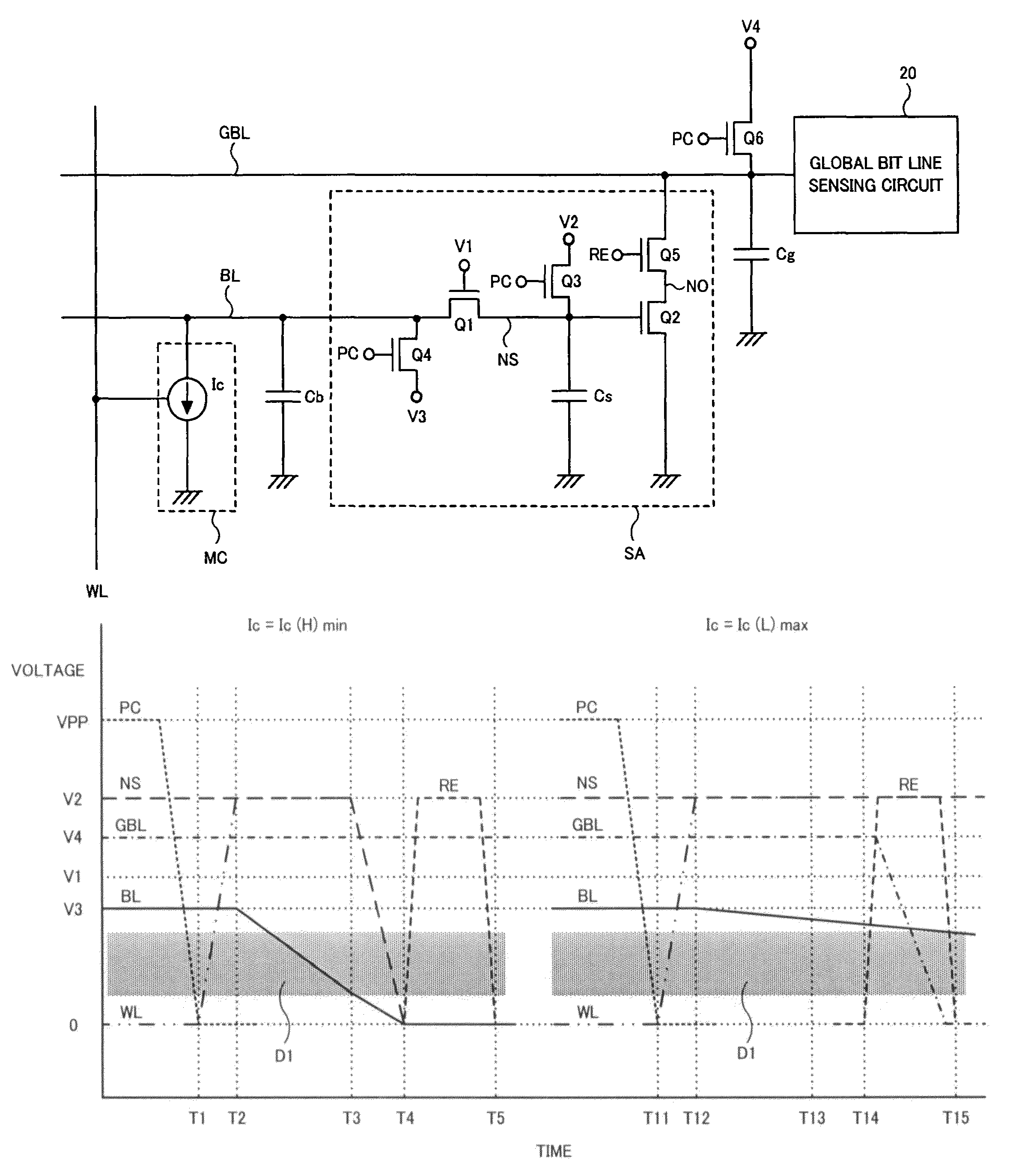
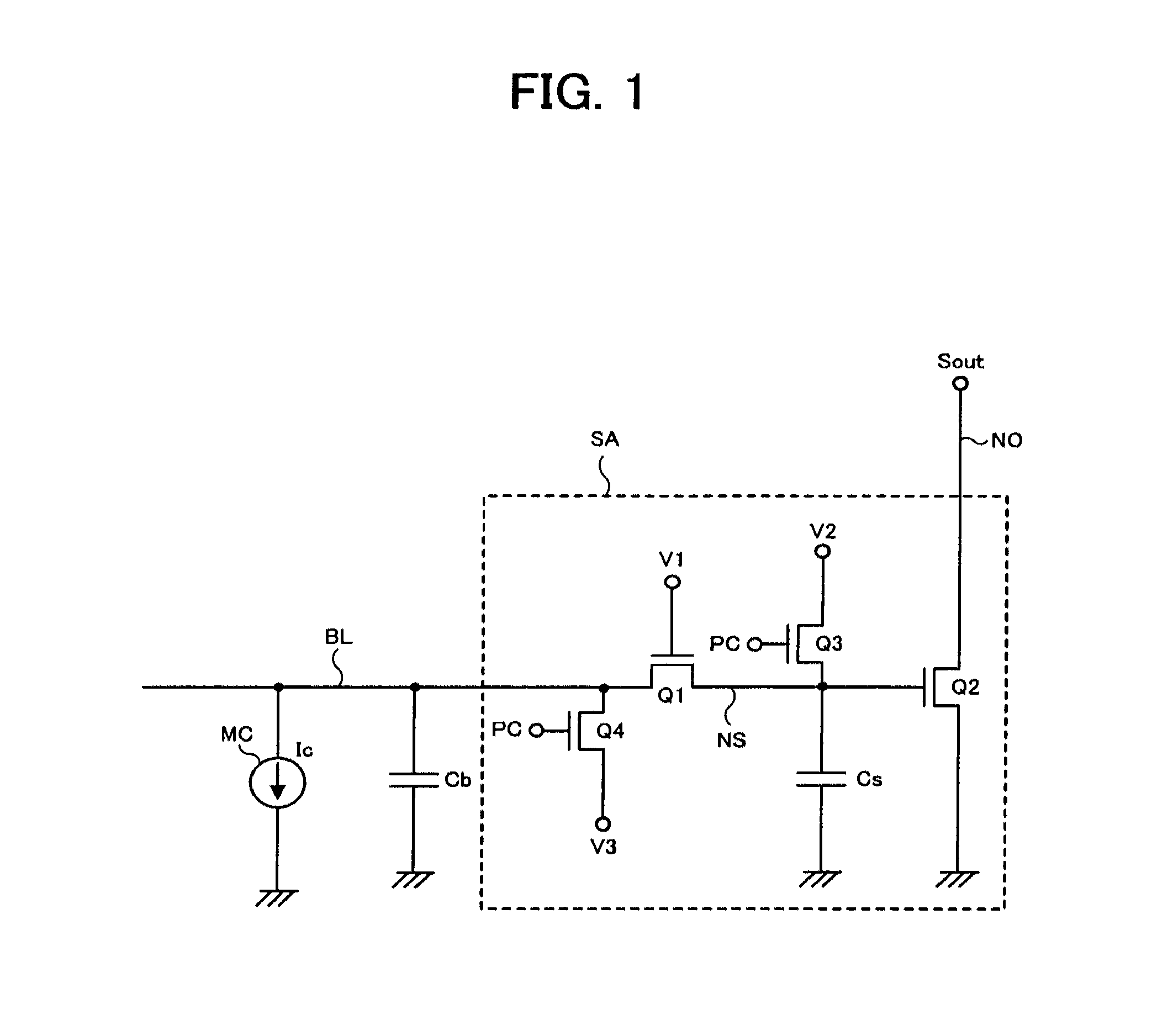
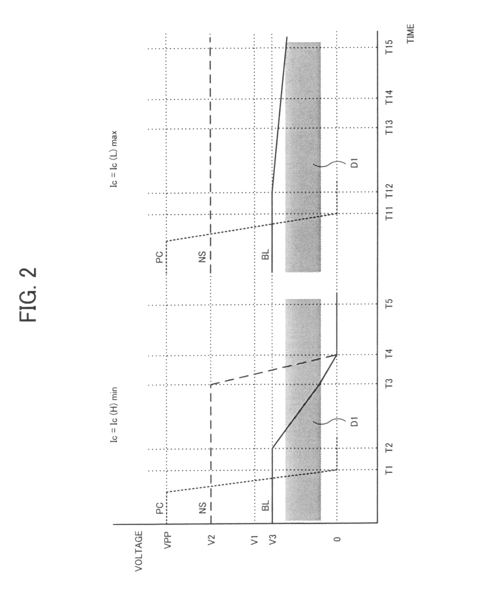
[0041]In a first embodiment, the invention is applied to a semiconductor device having current change memory cells, which comprises a memory cell array having a hierarchical bit line structure. FIG. 3 is a block diagram showing an entire configuration of the semiconductor device of the first embodiment. The semiconductor device shown in FIG. 3 comprises a memory cell array 10 including a large number of current change memory cells MC arranged at intersections of a plurality of word lines WL and a plurality of bit lines BL, and row circuits 11 and column circuits 12 that are attached to the memory cell array 10. The row circuits 11 includes a large number of circuits provided corresponding to the plurality of word lines WL, and the column circuits 12 includes a large number of circuits provided corresponding to the plurality of bit lines BL. In addition, since the memory cell array 10 employs the hierarchical bit line structure, the bit lines BL are hierarchized into global bit lines...

second embodiment

[0060]In a second embodiment, the invention is applied to a semiconductor device comprising a memory cell array having the hierarchical bit line structure, similarly as in the first embodiment. However, the second embodiment is different from the first embodiment in that potential control for the sense amplifier SA is modified. Here, the entire configuration of the semiconductor device of the first embodiment (FIG. 3) is common to the second embodiment, so description thereof will be omitted. FIG. 9 shows a configuration example in a range including the sense amplifier SA and the memory cell MC in the semiconductor device of the second embodiment. In the semiconductor device of FIG. 9, it is different from FIG. 4 of the first embodiment in that a transfer control voltage CT is applied to the gate terminal of the transistor Q1 instead of the potential V1. The transfer control voltage CT is set to either the potential V1 or the ground potential by the voltage control circuit 18a, as d...

third embodiment

[0066]In a third embodiment, the invention is applied to a semiconductor device comprising a memory cell array having the hierarchical bit line structure, similarly as in the first embodiment. However, a configuration of the third embodiment is partially modified from that of the first embodiment. Here, the entire configuration of the semiconductor device of the first embodiment (FIG. 3) is common to the third embodiment, so description thereof will be omitted. FIG. 11 shows a configuration example in a range including the sense amplifier SA and the memory cell MC in the semiconductor device of the third embodiment. In the semiconductor device of FIG. 11, it is different from FIG. 4 of the first embodiment in that an NMOS type transistor Q7 is added to the sense amplifier SA and that the global bit line sensing circuit 20 is replaced with a global bit line sensing / writing circuit 21.

[0067]The transistor Q7 for write control has a gate terminal to which a write control signal WE is a...


PUM


Abstract

A semiconductor device comprises a first transistor connected between a bit line and a sense node, and a second transistor amplifying a signal of the sense node. A first potential applied to a gate of the first transistor, a second potential supplied to the sense node, and a third potential supplied to the bit line are controlled so that the first potential applied to a gate of the first transistor is between the second and third potentials, the second potential is set larger than the third potential, and a predetermined potential obtained by subtracting a threshold voltage of the first transistor from the first potential is smaller than the third potential and higher than a low potential supplied to the second transistor. A potential of the bit line transitions from the third potential toward the low potential in accordance with data of a current change memory cell.

Description

BACKGROUND OF THE INVENTION[0001]1. Field of the Invention[0002]The invention relates to a semiconductor device comprising a single-ended sense amplifier circuit amplifying data that is stored in a current change memory cell and is read out to a bit line.[0003]2. Description of Related Art[0004]A current change memory cell has been conventionally known, which stores data in accordance with an amount of current flowing through a selected memory cell. In a semiconductor device using this type of memory cell, it is desirable to employ a single-ended sense amplifier having a small circuit scale instead of a differential type sense amplifier in terms of shrinking chip area. Further, miniaturization of the memory cell requires a low voltage operation, in which it is desirable to supply a potential as low as possible to the bit line connected to the memory cell.[0005]For example, Patent Reference 1 discloses a semiconductor device having memory cells each storing data in accordance with a ...

Claims


Application Information

Patent Timeline
Patent Type & Authority Patents(United States)
IPC IPC(8): G11C7/00
CPCG11C7/067G11C7/12G11C7/18G11C27/028
Inventor KAJIGAYA, KAZUHIKO
Owner LONGITUDE LICENSING LTD
Why Eureka
Try Eureka