Thin film transistor, and active matrix substrate and display device provided with such thin film transistor

A technology for thin film transistors and substrates, applied in transistors, electric solid state devices, semiconductor devices, etc., can solve problems such as the degradation of display quality, and achieve the effect of improving current driving capability

Inactive Publication Date: 2009-02-25
SHARP KK
View PDF3 Cites 12 Cited by
  • Summary
  • Abstract
  • Description
  • Claims
  • Application Information

AI Technical Summary

Problems solved by technology

However, simply making the gate insulating film thinner increases the capacitance (referred to as "parasitic capacitance") formed at the intersection of the scanning line and the signal line, which degrades the display quality.

Method used


Image

  • Thin film transistor, and active matrix substrate and display device provided with such thin film transistor
  • Thin film transistor, and active matrix substrate and display device provided with such thin film transistor
  • Thin film transistor, and active matrix substrate and display device provided with such thin film transistor

Examples


Embodiment approach 1

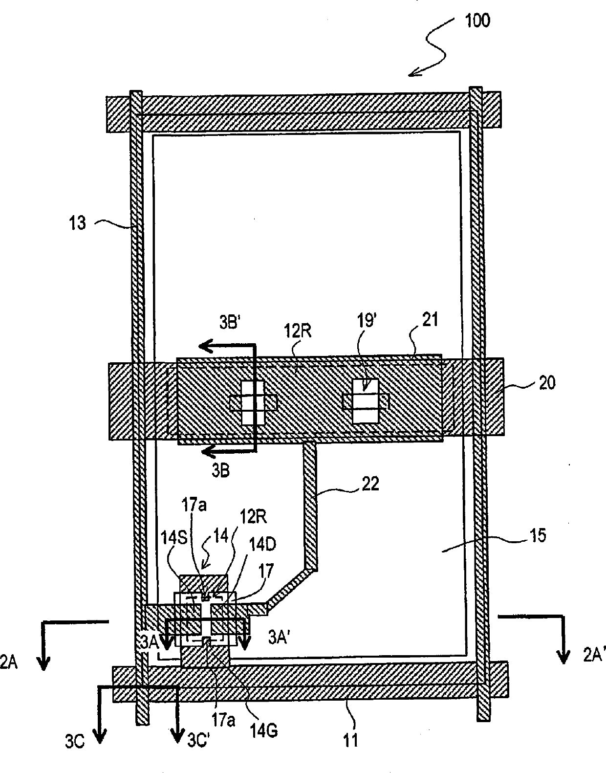
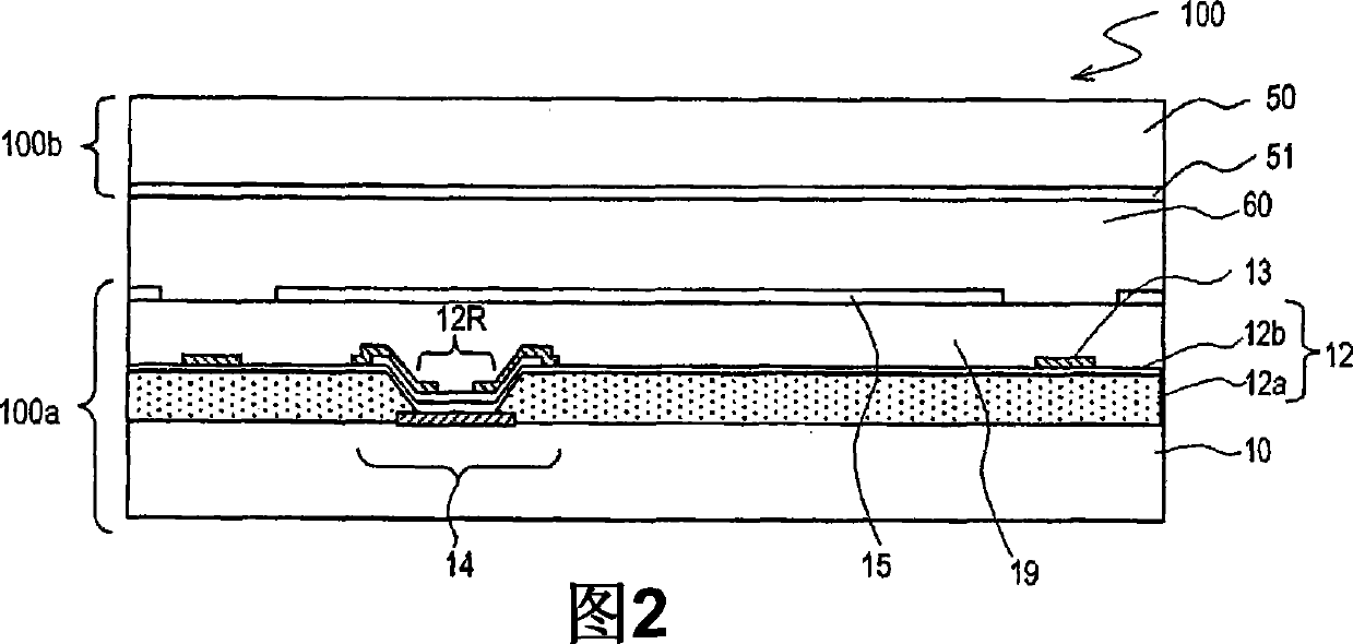
[0074] figure 1 2 and 2 show the liquid crystal display device 100 of this embodiment. figure 1 is a plan view schematically showing one pixel region of the liquid crystal display device 100, and FIG. 2 is along the figure 1 The cross-sectional view of line 2A-2A' in.

[0075] The liquid crystal display device 100 includes an active matrix substrate (hereinafter referred to as a "TFT substrate") 100a, an opposing substrate (also referred to as a "color filter substrate") 100b opposed to the TFT substrate 100a, and interposed therebetween. Liquid crystal layer 60 .

[0076] The TFT substrate 100a has a transparent insulating substrate (for example, a glass substrate) 10, a plurality of scanning wirings 11 formed on the substrate 10, an insulating film 12 covering these scanning wirings 11, and multiple scanning wirings 11 crossing the insulating film 12. signal wiring 13 .

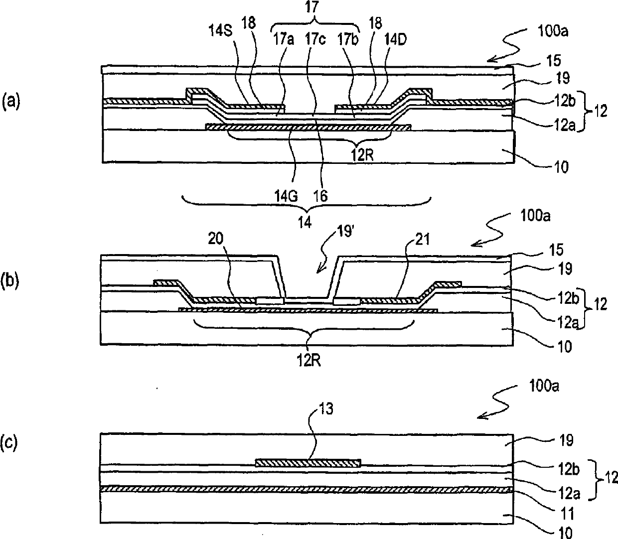
[0077] The TFT substrate 100a further has, in each pixel region: a thin film transistor (TFT) 14 tha...

Embodiment approach 2

[0122] Figure 13 and Figure 14 A thin film transistor (TFT) 14 of this embodiment is schematically shown. In the TFT 14 of the present embodiment, as Figure 13 and Figure 14 As shown, the channel region 17c is formed in an L-shape.

[0123] Also in the L-shaped TFT 14 having such a structure, by covering the edge of the gate electrode 14G with the first insulating layer 12a, the occurrence of leakage between the source electrode / drain electrode and the gate electrode can be suppressed.

[0124] In addition, by setting the relative arrangement relationship between the semiconductor layer 17 and the low-stack region 12R so that the current path always passes through the portion of the semiconductor layer 17 above the low-stack region 12R, an effect of improving the off characteristic can be obtained. For example, in Figure 13 In the shown structure, by forming the low stack region 12R in an L-shape, the width of the low stack region 12R along the channel width directio...

Embodiment approach 3

[0127] Figure 15 and Figure 16 The TFT 14 of this embodiment is schematically shown. The TFT14 of this embodiment, such as Figure 15 and Figure 16 As shown, there are two drain electrodes 14D, and a source electrode 14S is arranged between these two drain electrodes 14D. When such a structure is adopted, even if the alignment shift of the photomask occurs, the change in the gate-drain capacitance can be canceled between the two drain electrodes 14D, so the gate-drain capacitance as a whole of the TFT 14 can be suppressed. change in capacitance.

[0128] In the TFT 14 having such a structure, by covering the edge of the gate electrode 14G with the first insulating layer 12a, the occurrence of leakage between the source / drain layer and the gate electrode layer can be suppressed. In addition, by setting the relative arrangement relationship between the semiconductor layer 17 and the low stack region 12R so that the current path always passes through the portion of the se...


PUM


Abstract

The invention provides a film transistor and a source matrix substrate with the film transistor and the display device. The invention improves the electric current driving capability of a thin film transistor without the yield being decreased due to a defective leak between a source electrode / drain electrode and a gate electrode or due to a decrease in an off-characteristic. A thin film transistor according to the present invention includes a gate electrode; an insulating film covering the gate electrode; a semiconductor layer provided on the insulating film; and a source electrode and a drain electrode provided on the insulating film and the semiconductor layer. The insulating film is a multiple layer insulating film including a first insulating layer and a second insulating layer provided on the first insulating layer. The multiple layer insulating film has a low stacking region excluding the first insulating layer and a high stacking region in which the first insulating layer and the second insulating layer are stacked. The first insulating layer is provided so as to cover at least an edge of the gate electrode. The semiconductor layer is provided on both the low stacking region and the high stacking region of the multiple layer insulating film. The semiconductor layer and the low stacking region are arranged such that a path of a current flowing between the source electrode and the drain electrode necessarily passes a part of the semiconductor layer which is located above the low stacking region.

Description

technical field [0001] The present invention relates to thin film transistors. In addition, the present invention also relates to an active matrix substrate and a display device including thin film transistors. Background technique [0002] Liquid crystal display devices are characterized by thinness and low power consumption, and are widely used in various fields. In particular, an active matrix type liquid crystal display device including a thin film transistor (referred to as "TFT") in each pixel has high contrast and excellent response characteristics, and high performance, so it is used in televisions, monitors In recent years, its market size is expanding. [0003] On an active matrix substrate used in an active matrix liquid crystal display device, a plurality of scanning wirings and a plurality of signal wirings intersecting these scanning wirings through an insulating film are formed. , are provided with thin film transistors for driving pixels. [0004] In rece...

Claims


Application Information

Patent Timeline
Patent Type & Authority Applications(China)
IPC IPC(8): H01L29/786H01L21/336
CPCH01L27/1214H01L29/78696H01L29/42384H01L29/41733H01L27/1248H01L29/78609H01L27/12H01L29/4908
Inventor 冈田美广中村涉伴厚志
Owner SHARP KK
Why Eureka
Try Eureka