
Vertical 8F2 cell dram with active area self-aligned to bit line

a cell and active area technology, applied in the field of memory devices, can solve the problems of inability to fill the trench properly without, the deep trench cannot be too small, and the actual design and implementation of such cells typically requires a highly complex dram design and process technology, so as to increase the space available for the deep trench region

Inactive Publication Date: 2005-04-26
POLARIS INNOVATIONS
View PDF11 Cites 8 Cited by
  • Summary
  • Abstract
  • Description
  • Claims
  • Application Information

AI Technical Summary

Benefits of technology

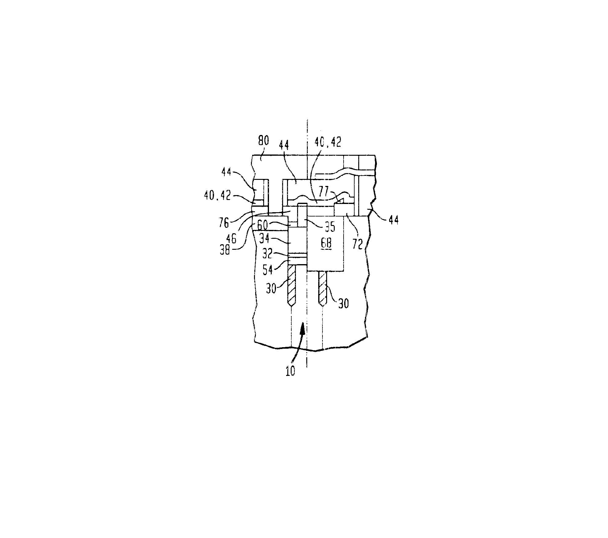
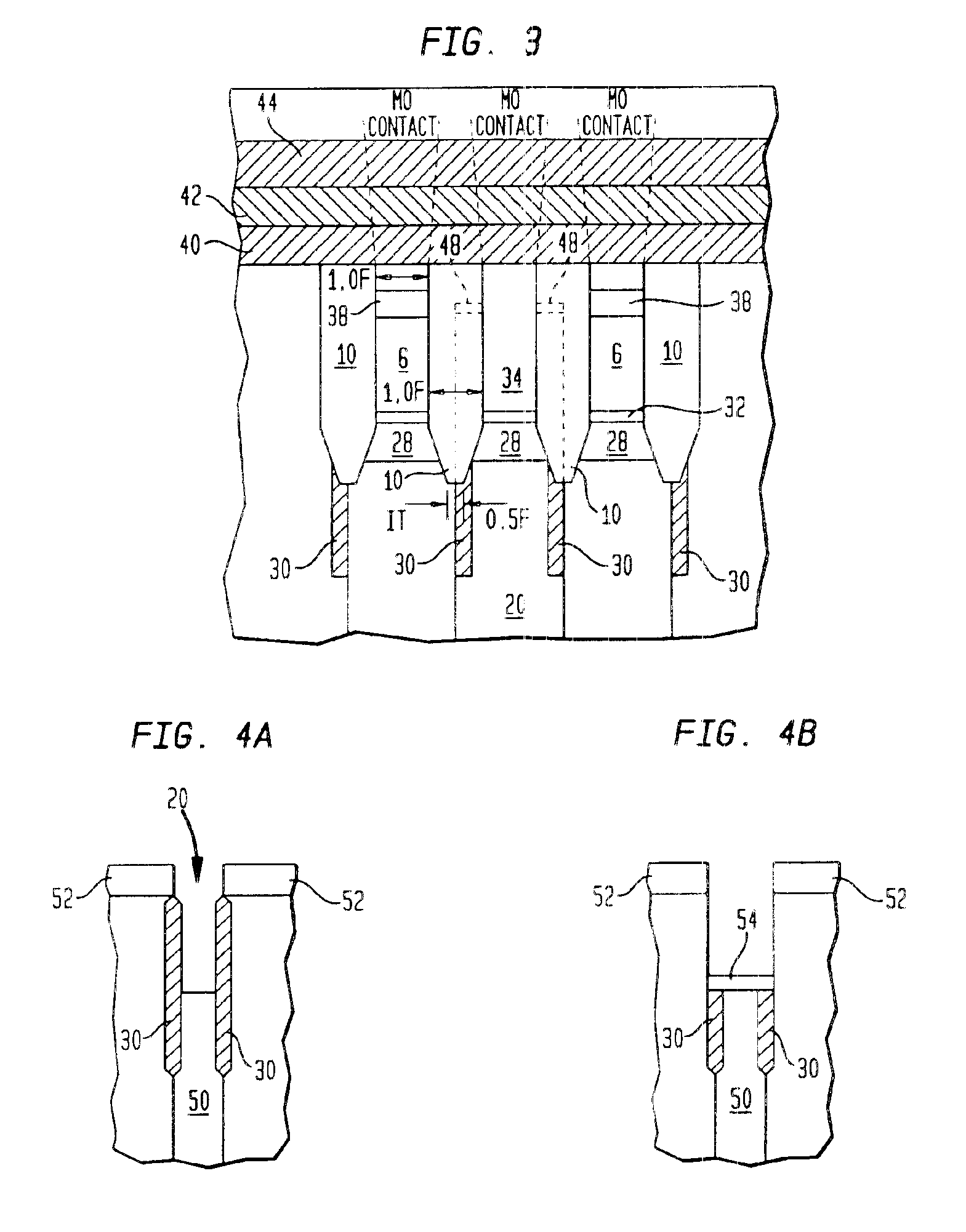
[0015]The present invention provides a 8F2 vertical DRAM cell in which the bit line structure is formed prior to the etching of the isolation trench and the formation of the word line structure, and the bit line structure is then used to mask the etching of the isolation trench so that the active area is self-aligned to the bit line, thereby increasing the space available for the deep trench region.

Problems solved by technology

Though the DRAM memory cell is based on simple concepts, the actual design and implementation of such cells typically requires a highly complex DRAM design and process technology.
However, the deep trench cannot be made too small or the trench cannot be filled properly without the presence of voids.
As a result, the etch step that forms the deep trench becomes increasingly difficult to control within desired specifications.
Moreover, as these devices become smaller, the trench collar oxide layer that is located along the sidewalls of the deep trenches cannot be formed using existing localized oxidation of silicon (LOCOS) processes and must be formed, instead, by a buried collar or other costly process steps.
Additionally, with such devices, voids may be present in the high-density plasma (HDP) deposited oxide or other dielectrics that are typically used to fill the isolation trenches.
Further, two bit line contacts are typically present for each deep trench, resulting in a significant increase in the bit line capacitance.

Method used


Image

  • Vertical 8F2 cell dram with active area self-aligned to bit line
  • Vertical 8F2 cell dram with active area self-aligned to bit line
  • Vertical 8F2 cell dram with active area self-aligned to bit line

Examples


Embodiment Construction

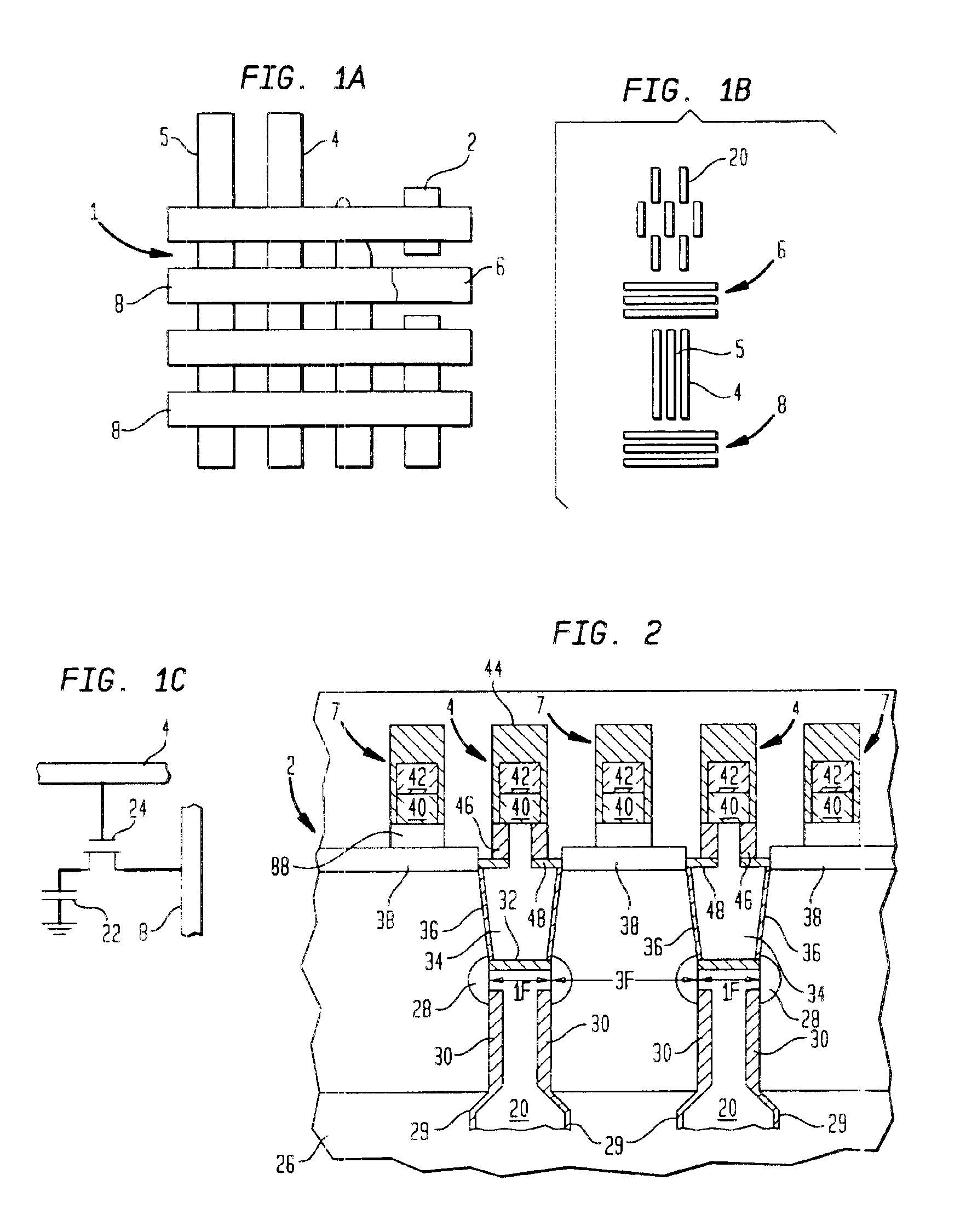
[0040]FIGS. 1A and 1B illustrate, in plan view, a known 8F2 DRAM memory cell array comprised of plural memory cells. Examples of such known 8F2 DRAM cells and processes for fabricating such DRAM cells are described in U.S. application Ser. No. 09 / 888,202, filed Jun. 22, 2001, the disclosure of which is incorporated herein by reference.

[0041]FIG. 1A shows various mask patterns of a known memory cell array superimposed on one another. FIG. 1B shows each mask pattern of FIG. 1A separately, namely FIG. 1B represents the view of FIG. 1A at four different depths. The topmost pattern of FIG. 1B illustrates an arrangement of a plurality of deep trenches 20. The second pattern from the top in FIG. 1B illustrates the arrangement of the known active areas in which doped junctions used for pass transistors are formed. The third pattern from the top illustrates the arrangement of the gate contact patterns or word lines of the cell array, and the bottom pattern illustrates the arrangement of the ...


PUM


Abstract

A memory cell is formed in a memory cell array comprised of a plurality of memory cells arranged in rows and columns. A deep trench structure is formed within a semiconductor substrate and includes at least one conducting region. A patterned bit line structure is formed atop of, and electrically isolated from, the insulating region of the deep trench structure and atop of, but contacting at least part of, regions of the semiconductor substrate. Exposed portions of the semiconductor substrate are etched to form at least one isolation trench adjoining the deep trench structure using the patterned bit line structure as an etch mask. The isolation trench is filled with a dielectric material. A contact region to the conducting region of the deep trench structure is formed within the dielectric material of the isolation trench and is electrically isolated from the bit line structure. A word line structure that connects to the contact region is formed and is at least partly atop of, but electrically isolated from, the bit line structure.

Description

BACKGROUND OF THE INVENTION[0001]The present invention is directed to memory devices and, more particularly, to dynamic random access memory (DRAM) structures formed in a substrate.[0002]Dynamic random access memory devices (DRAMs) typically include a semiconductor memory cell array formed of a plurality of memory cells arranged in rows and columns and include a plurality of bit lines as well as a plurality of word lines that intersect the bit lines. Each memory cell of the array is located at the intersection of a respective word line and a respective bit line and includes a capacitor for storing data and a transistor for switching, such as a planar or vertical MOS transistor. The word line is connected to the gate of the switching transistor, and the bit line is connected to the source or drain of the switching transistor. When the transistor of the memory cell is switched on by a signal on the word line, a data signal is transferred from the capacitor of the memory cell to the bi...

Claims


Application Information

Patent Timeline
IPC IPC(8): H01L21/70H01L21/8242H01L27/108
CPCH01L27/10864H01L27/10891H01L27/10888H01L27/10876H10B12/0383H10B12/053H10B12/488H10B12/485
Inventor ARNOLD, NORBERTJAIPRAKASH, VENKATACHALAM C.
Owner POLARIS INNOVATIONS
Learn More