Electromagnetic shield film, electromagnetic shield unit and display

a technology of electromagnetic shielding and electromagnetic shielding film, which is applied in the field of electromagnetic shielding film, electromagnetic shield unit and display, can solve the problems of increasing electromagnetic wave-related problems, increasing the number of electromagnetic shielding films, so as to improve the electromagnetic shielding performance, prevent the earth portion from being creased, and improve the effect of electromagnetic shielding performan

Inactive Publication Date: 2005-04-26
HITACHI CHEM CO LTD
View PDF10 Cites 69 Cited by
  • Summary
  • Abstract
  • Description
  • Claims
  • Application Information

AI Technical Summary

Benefits of technology

[0017]The non-conductive region enables the conductive region to freely expand and contract, and prevent the earth portion from being creased.
[0042]This display also includes an earth portion with the conductive and non-conductive regions and in which the conductive region can freely expand and contract. This is effective in preventing the earth portion from being creased, and in improving the electromagnetic wave shielding performance and promoting mass production.

Problems solved by technology

Electromagnetic waves radiated from electric and electronic devices have become one of serious social problems.
Such electromagnetic waves tend to reach adjacent devices as noise or erroneously operate them.
As more electric and electronic devices are used and computers are used to control such electric and electronic devices, electromagnetic wave-related problems increase and inevitably become more serious and unpredictable.
Further, it is pointed out that electromagnetic waves result in health hazard.
However, the foregoing measures tend to adversely affect the most important feature, i.e. visibility of images on the display.
In the foregoing case, it is very difficult to smoothly and uniformly bond the conductor and the earth portion on the transparent base.
Air bubbles are sometimes present between the transparent base and the conductor and between the transparent base and the earth portion, which causes non-uniform or insufficient bonding.
To overcome this problem, it is conceivable to use a very strong adhesive, which might put a limit on productivity or adversely affect mass productivity.
Further, if the electromagnetic wave shield filter is directly integrated to a display cabinet or to a display body, it is also very difficult to bond the transparent base and conductive members smoothly and reliably.
Air bubbles may be present between the transparent base and the conductive members, which will cause partial contact or bonding thereof.
This will reduce electromagnetic wave shielding performance and damage the display body.

Method used


Image

  • Electromagnetic shield film, electromagnetic shield unit and display
  • Electromagnetic shield film, electromagnetic shield unit and display
  • Electromagnetic shield film, electromagnetic shield unit and display

Examples


first example

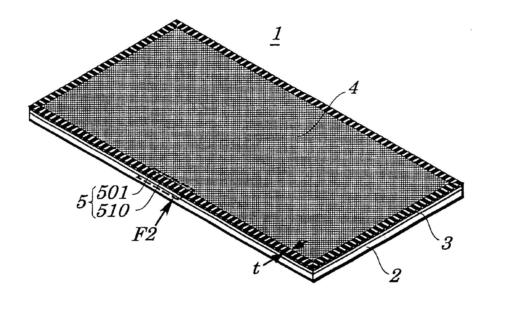
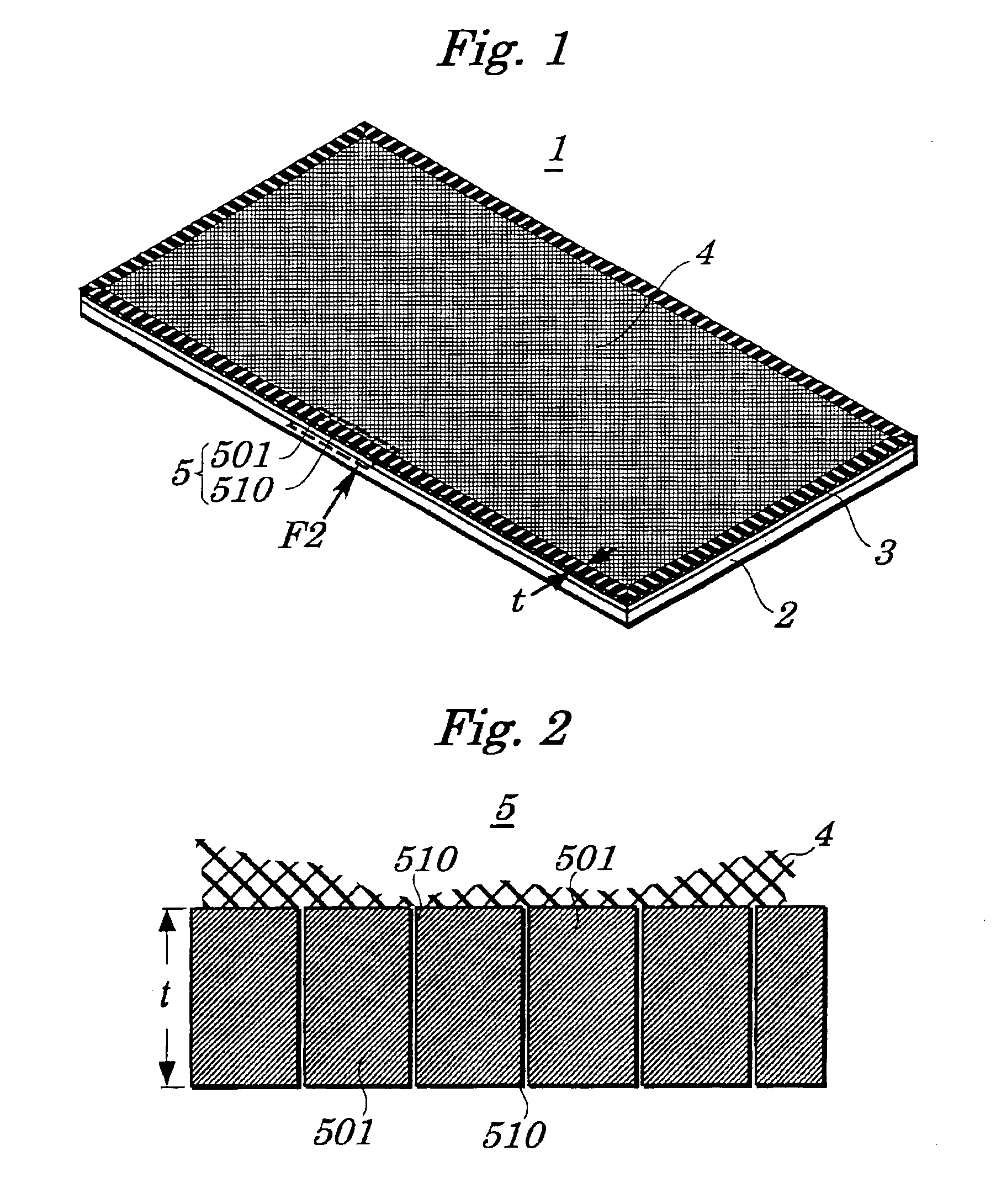
[0129]The transparent base 2 is a 100 μm thick polyethylene terephthalate (PET) film (brand name “EMBLET S” manufactured by Unitika Ltd.), and the adhesive 3 is a polyester resin (brand name “BYRON UR-1400” manufactured by Toyo Boseki Kabushiki Kaisha). The adhesive 3 is applied onto the transparent base 2 using a painting machine at a room temperature so that the adhesive 3 is 30 μm thick when dried. A 18 μm thick copper foil (brand name “BHY-22B-T” manufactured by Japan Energy, Ltd.) is roll-laminated onto the transparent base 2 in order to make the conductor 4 and the conductive regions 501 under conditions of 150° C. and 196×104 Pa. In this case, a coarse surface of the copper foil is in contact with the adhesive 3. A film on which the conductor 4 and conductive regions 501 are laminated is obtained.

[0130]A mesh geometric pattern which has a line width of 25 μm and a line space of 250 μm is made on the conductor 4 by the photolithographic process. Further, the mesh geometric pat...

second example

[0132]The forgoing conditions are applied in order to make conductor 4 with the mesh geometric pattern, the earth portion 5 having the conductive regions 501 with the rectangular geometric pattern (shown in FIG. 18) and the non-conductive regions 510 in the shape of a slit. The earth portion 5 of FIG. 18 is identical to the earth portion 5 having the first structure, shown in FIG. 2. In this example, the conductive region 501 has a length L2 of 100 mm while the slit width W2 is 5 mm.

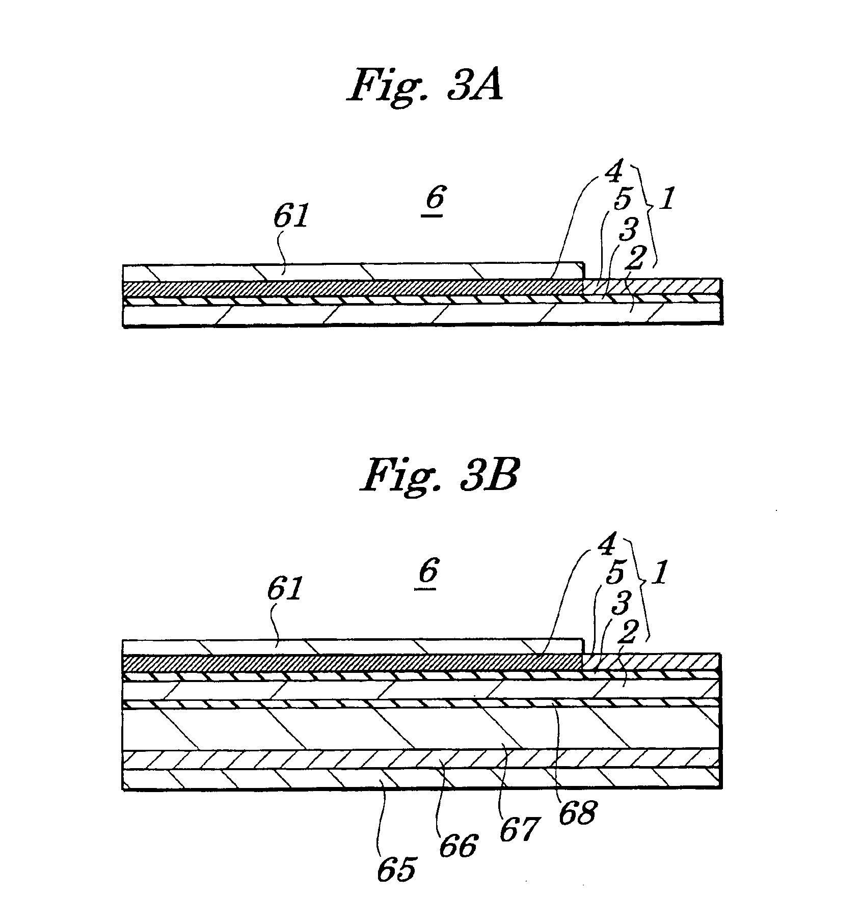
[0133]As described in the first example, after the chemical etching, the surface of the adhesive 3 becomes opaque because the coarse surface of the copper foil has been transferred thereto. In order to obtain the transparent electromagnetic wave shield film 1 having the second structure, the surface of the copper foil on the conductive regions 501 and the adhesive PET film as the adhesive 3 are heated and pressed under the conditions of 120° C. and 49×104 Pa.

third example

[0134]The conditions mentioned in the first example are also applied in this example. The conductor 4 has the mesh geometric pattern while the earth portion 5 includes the comb-shaped conductive regions 501 and the slit-shaped non-conductive regions 510, as shown in FIG. 19. The earth portion 5 shown in FIG. 19 is identical to the earth portion 5 having the third structure shown in FIG. 10. The length L3 of the conductive region 501 is 100 mm, the slit width W3 is 5 mm, and the length t1 of the non-conductive region 510 is 2 mm.

[0135]After the chemical etching, the surface of the adhesive 3 also becomes opaque because the coarse surface of the copper foil has been transferred thereto. In order to obtain the transparent electromagnetic wave shield film 1 having the second structure, the surface of the copper foil on the conductive regions 501 and the adhesive PET film as the adhesive 3 are heated and pressed under the conditions of 120° C. and 49×104 Pa.


PUM


Abstract

An electromagnetic wave shield film (1) comprises a transparent base (2), a conductor (4) positioned on the transparent base (2) via an adhesive (3) and having a mesh geometric pattern, and an earth portion (5) arranged around the conductor (4) and including conductive regions (501) which absorb electromagnetic waves, and non-conductive regions (510) which prevent the earth portion (5) from being creased.

Description

TECHNICAL FIELD[0001]The present invention relates to an electromagnetic wave shield film, an electromagnetic wave shield unit and a display, and more particularly relates not only to an electromagnetic wave shield film which shields electromagnetic waves generated via a front part of a plasma display including a plasma display panel (PDP), a cathode ray tube (CRT) display, a liquid crystal display (LC), an electro luminescence display (EL) or the like, but also to an electromagnetic wave shield unit including the electromagnetic wave shield film and a display including the electromagnetic wave shield unit.BACKGROUND ART[0002]Recently, computerization has been remarkably promoted and improved. Displays are one of essential items for the computerization, and are being used for a variety of devices such as television sets (TV), word processors, personal computers, analyzers, game machines, and vehicle-mounted monitors. Further, such displays have been extensively enlarged.[0003]Electr...

Claims


Application Information

Patent Timeline
Patent Type & Authority Patents(United States)
IPC IPC(8): H05K9/00
CPCH05K9/0096H05K9/00
Inventor TAKAHASHI, HIROAKIIMAIZUMI, JUNICHINAKAMURA, HAJIMENOMURA, HIROSHI
Owner HITACHI CHEM CO LTD
Why Eureka
Try Eureka