

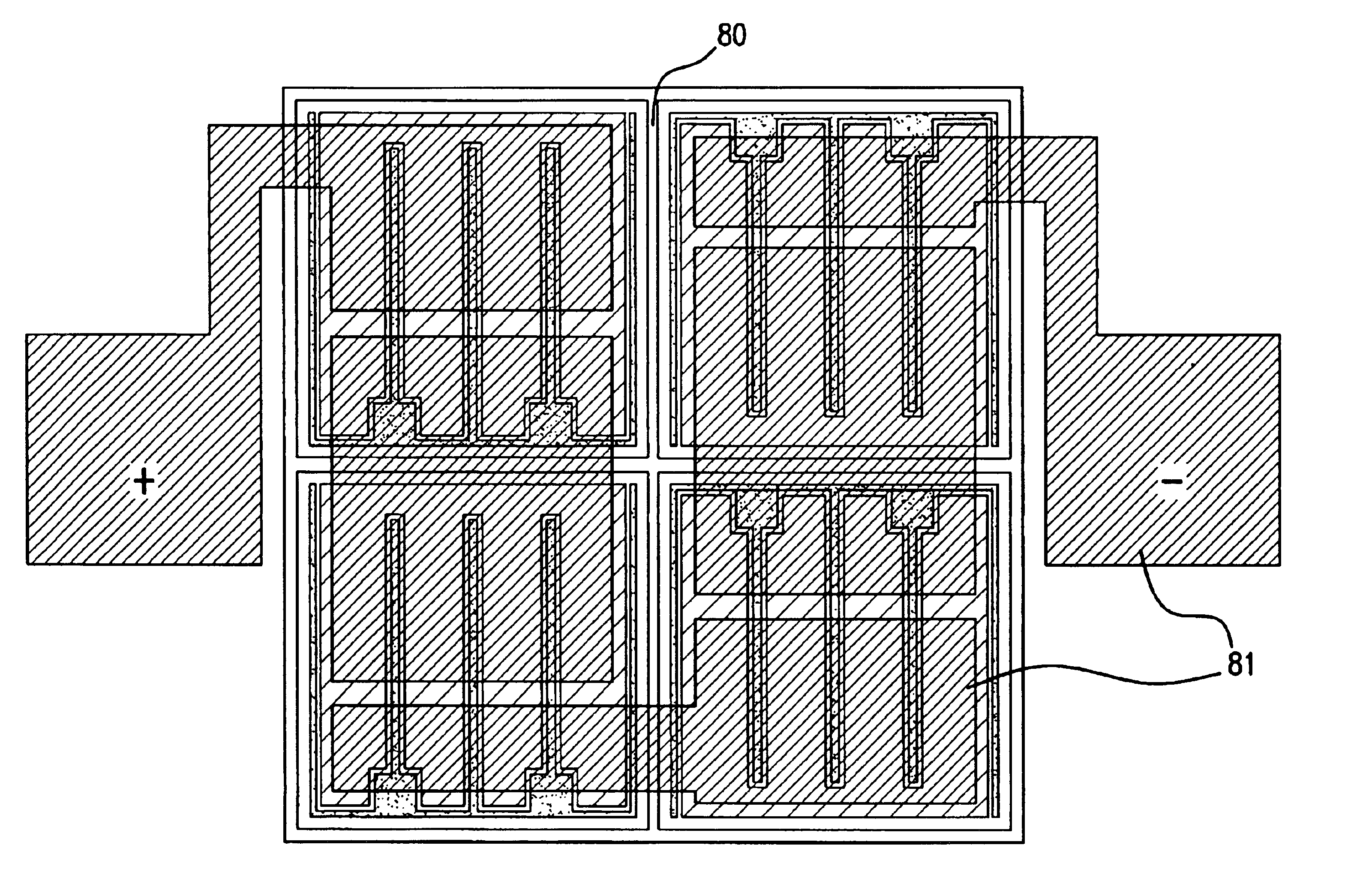
Multi-chip semiconductor LED assembly
a semiconductor led and chip technology, applied in semiconductor devices, instruments, electrical devices, etc., can solve the problems of spatially extensive structures and spatially extensive structures, and achieve the effect of improving light extraction
- Summary
- Abstract
- Description
- Claims
- Application Information
AI Technical Summary
Benefits of technology
Problems solved by technology
Method used
Image

Examples
Embodiment Construction
[0047]First, a detailed description of an inverted III-Nitride LED and a submount for one or more LEDs is provided, which corresponds to the disclosure in the parent application. In the second part of this application additional embodiments are described in detail, utilizing several inverted III-V LEDs mounted on a shared submount.
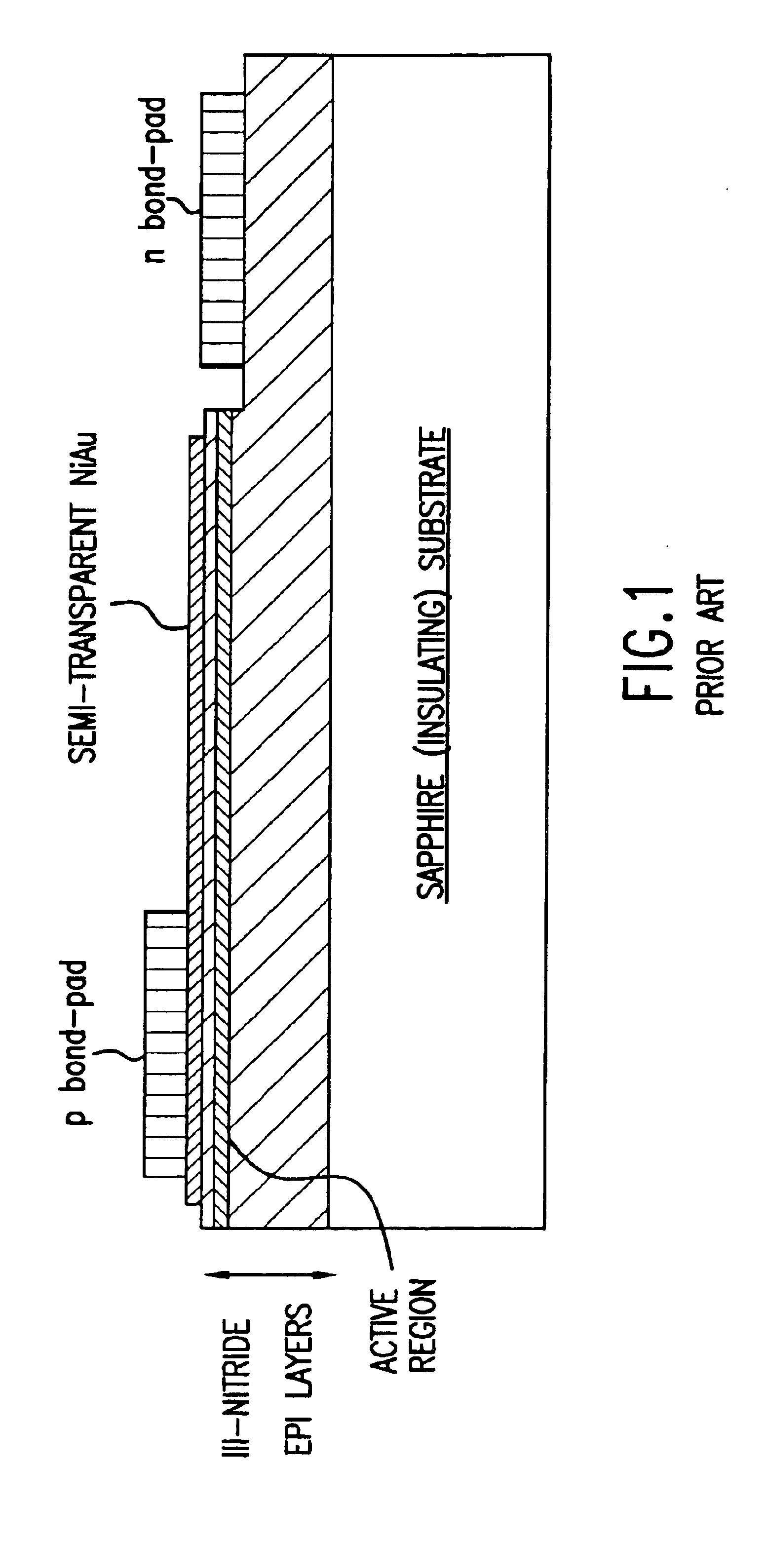
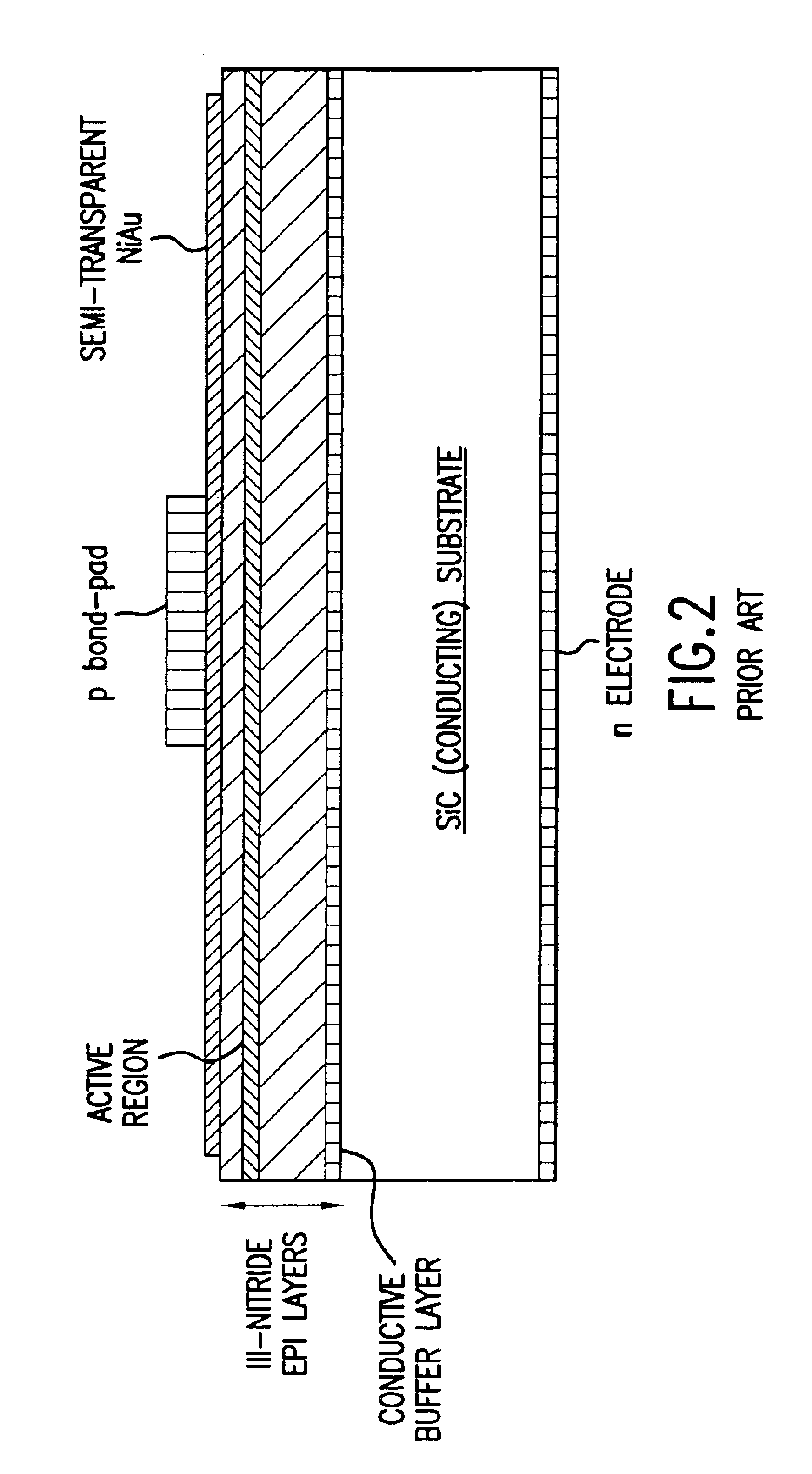
The Inverted III-Nitride LED
[0048]One fundamental limiting condition of LED operation is maximum junction temperature. The maximum junction temperature, Tjmax, is the temperature of the p-n junction region at which breakdown or failure occurs in some part of the LED or its housing. This breakdown often occurs as the glass transition temperature of an encapsulating epoxy or lens is approached, causing loss of transparency and eventual melting of these materials. With such a limit established, ΔTj, the temperature rise from ambient to Tjmax, may be expressed as (assuming power conversion efficiency <<100% which is true for present-day III-nitride devices),
ΔT...
PUM
 Abstract
Description
Claims
Application Information