Non-volatile semiconductor memory device and process for fabricating the same

a semiconductor memory and non-volatile technology, applied in the direction electrical appliances, transistors, etc., can solve the problems of disadvantageous poor transistor properties of semiconductor memory devices, and the inability to perform the operation of recording 2 bits per unit memory devices, etc., to achieve no deterioration in properties

Inactive Publication Date: 2005-04-26
SONY CORP
View PDF2 Cites 52 Cited by
  • Summary
  • Abstract
  • Description
  • Claims
  • Application Information

AI Technical Summary

Benefits of technology

[0029]The non-volatile semiconductor memory device of the present invention suffers almost no deterioration in the properties and can perform the operation of recording of 2 bits per unit memory device even when the s

Problems solved by technology

However, the shortening of the gate length causes a so-called short channel effect, and typically, when the gate length is 0.1 μm or shorter, the transistor properties of the semiconductor memory device disadvantageously become poor.
In addition, in the above-mentioned semiconductor memory device in which a channel is formed in the semiconductor substrate and electrons are locally written in the source end or the drain end in the discrete charge s

Method used


Image

  • Non-volatile semiconductor memory device and process for fabricating the same
  • Non-volatile semiconductor memory device and process for fabricating the same
  • Non-volatile semiconductor memory device and process for fabricating the same

Examples


first embodiment

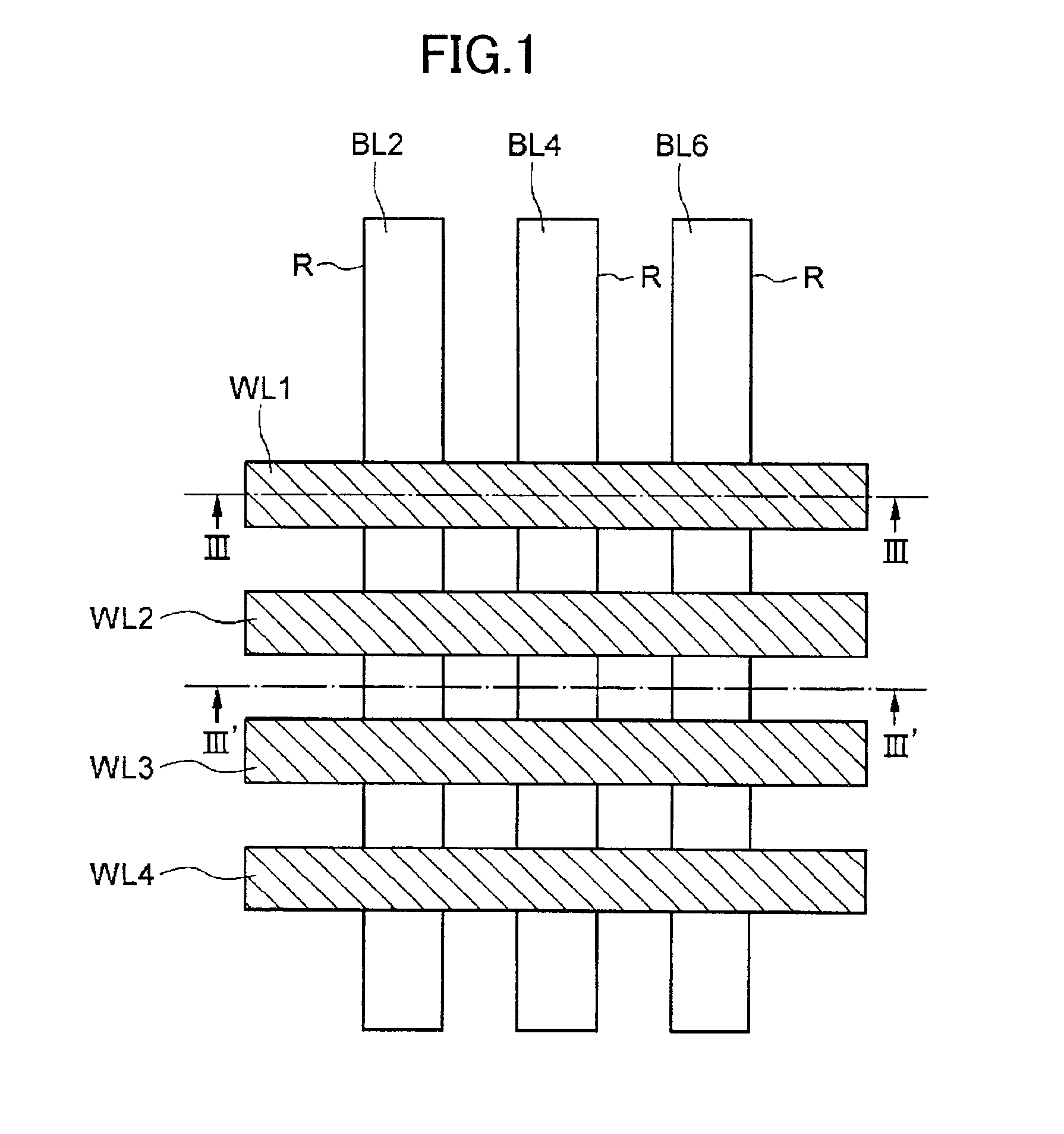
[0041]FIG. 1 is a diagrammatic plan view of a memory cell array according to the present embodiment. As shown in FIG. 1, trenches R are formed in a semiconductor substrate (including an SOI layer) in a stripe form at a predetermined interval, and word lines WL are formed in a stripe form in the direction perpendicular to the trenches R.

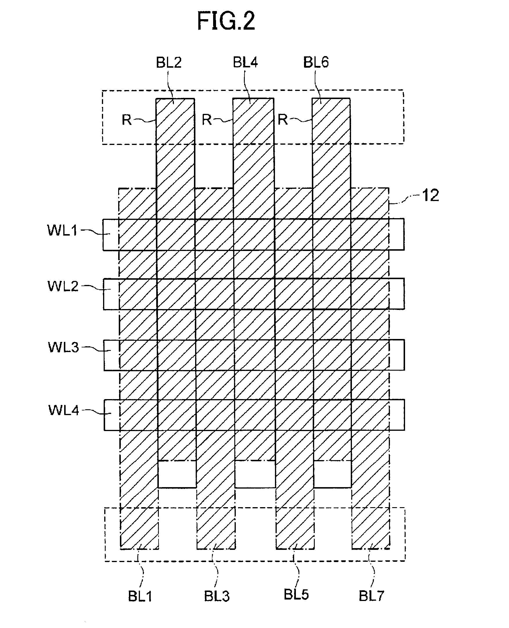
[0042]FIG. 2 is a diagrammatic view showing an impurity region formed on the semiconductor substrate shown in the plan view of FIG. 1. As shown in a shaded portion in FIG. 2 indicated by slant lines, an impurity region (source-drain region) 12 which functions as a source or a drain is formed, and the source-drain region 12 at the bottom portions of the trenches R formed in the semiconductor substrate forms bit lines BL2, BL4, BL6. The source-drain region 12 on the semiconductor substrate, in which no trench R is formed, forms bit lines BL1, BL3, BL5, BL7.

[0043]Thus, the bit lines BL comprised of the source-drain region 12 are arranged in parallel in o...

second embodiment

[0113]The present embodiment illustrates a non-volatile semiconductor memory device using, as charge storage means for the memory transistor, a number of conductors each having a particle diameter of, for example, 10 nm or less (hereinafter, referred to as “small particle-size conductors”), which are insulated from one another and embedded in the gate dielectric film.

[0114]FIG. 8 is an enlarged diagrammatic cross-sectional view showing a device structure of the memory transistor using small particle-size conductors as the charge storage means.

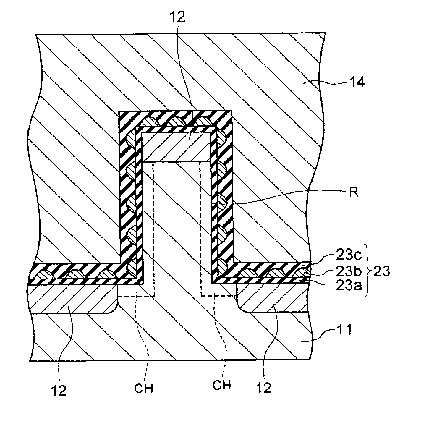
[0115]In the non-volatile memory transistor of the present embodiment, a gate dielectric film 23 comprises a bottom dielectric film 23a, small particle-size conductors 23b as charge storage means on the film 23a, and a dielectric film 23c which coats the small particle-size conductors 23b.

[0116]Other constituents, namely, the semiconductor substrate 11, the channel formation region CH, the source-drain region 12, and the gate electrode 14 are ...


PUM


Abstract

A non-volatile semiconductor memory device comprising a first conductive semiconductor having steps on a surface thereof, a second conductive semiconductor region formed on an upper portion and a bottom portion of each of the steps and being separated in a direction perpendicular to the main surface of the first conductive semiconductor to function as a source or a drain, a gate dielectric film containing therein charge storage means which is spatially discrete and being formed on the first conductive semiconductor so as to coat at least a sidewall of each of the steps, and a gate electrode formed on the gate dielectric film. Accordingly, there are provided a non-volatile semiconductor memory device which suffers almost no deterioration in the properties and can perform the operation of recording of 2 bits per unit memory device even when the size of the semiconductor memory device in the semiconductor substrate is scaled down, and a process for fabricating the non-volatile semiconductor memory device.

Description

CROSS REFERENCES TO RELATED APPLICATIONS[0001]The present document is based on Japanese Priority Document JP 2001-079123, filed in the Japanese Patent Office on Mar. 19, 2001, the entire contents of which being incorporated herein by reference.BACKGROUND OF THE INVENTION[0002]1. Field of the Invention[0003]The present invention relates to a non-volatile semiconductor memory device having charge storage means which is two-dimensionally discrete, for example, a charge trap in the nitride film in a metal oxide nitride oxide semiconductor (MONOS) type device or metal nitride oxide semiconductor (MNOS) type device, wherein the device records or erases data by injecting charges into or taking out charges from the charge storage means, and a process for fabricating the non-volatile semiconductor memory device.[0004]2. Description of the Related Art[0005]As non-volatile semiconductor memory devices, there are known floating gate (FG)-type memory devices in which a charge storage means (floa...

Claims


Application Information

Patent Timeline
IPC IPC(8): H01L21/70H01L27/115H01L29/66H01L21/8246H01L29/792H01L21/8247H01L29/788
CPCH01L27/115H01L29/792H01L27/11568Y10S438/954H10B69/00H10B43/30
Inventor NOMOTO, KAZUMASAKOBAYASHI, TOSHIO
Owner SONY CORP
Why Eureka
Try Eureka