Ferroelectric emitter

a ferroelectric emitter and emitter technology, applied in the manufacture of discharge tube/lamps, discharge tube main electrodes, electrode systems, etc., can solve the problems of requiring the restriction of re-polling an emitter, the isolated pattern such as doughnut shape, and the inability to guarantee electron emission of the conventional ferroelectric emitter. to achieve the effect of convenient separability

Inactive Publication Date: 2005-04-26
SAMSUNG ELECTRONICS CO LTD +1
View PDF10 Cites 6 Cited by
  • Summary
  • Abstract
  • Description
  • Claims
  • Application Information

AI Technical Summary

Benefits of technology

[0010]In a preferred embodiment of the present invention, the predetermined pattern is formed in the top surface of the dielectric layer excluding the two end portions thereof, an

Problems solved by technology

However, a conventional ferroelectric emitter cannot guarantee electron emission where the gap between two electrodes is too wide or too narrow for switching.
For example, in the conventional ferroelectric emitter, if the gap between two electrodes is too wide an electric field cannot reach the center portion of

Method used


Image

  • Ferroelectric emitter
  • Ferroelectric emitter
  • Ferroelectric emitter

Examples


Embodiment Construction

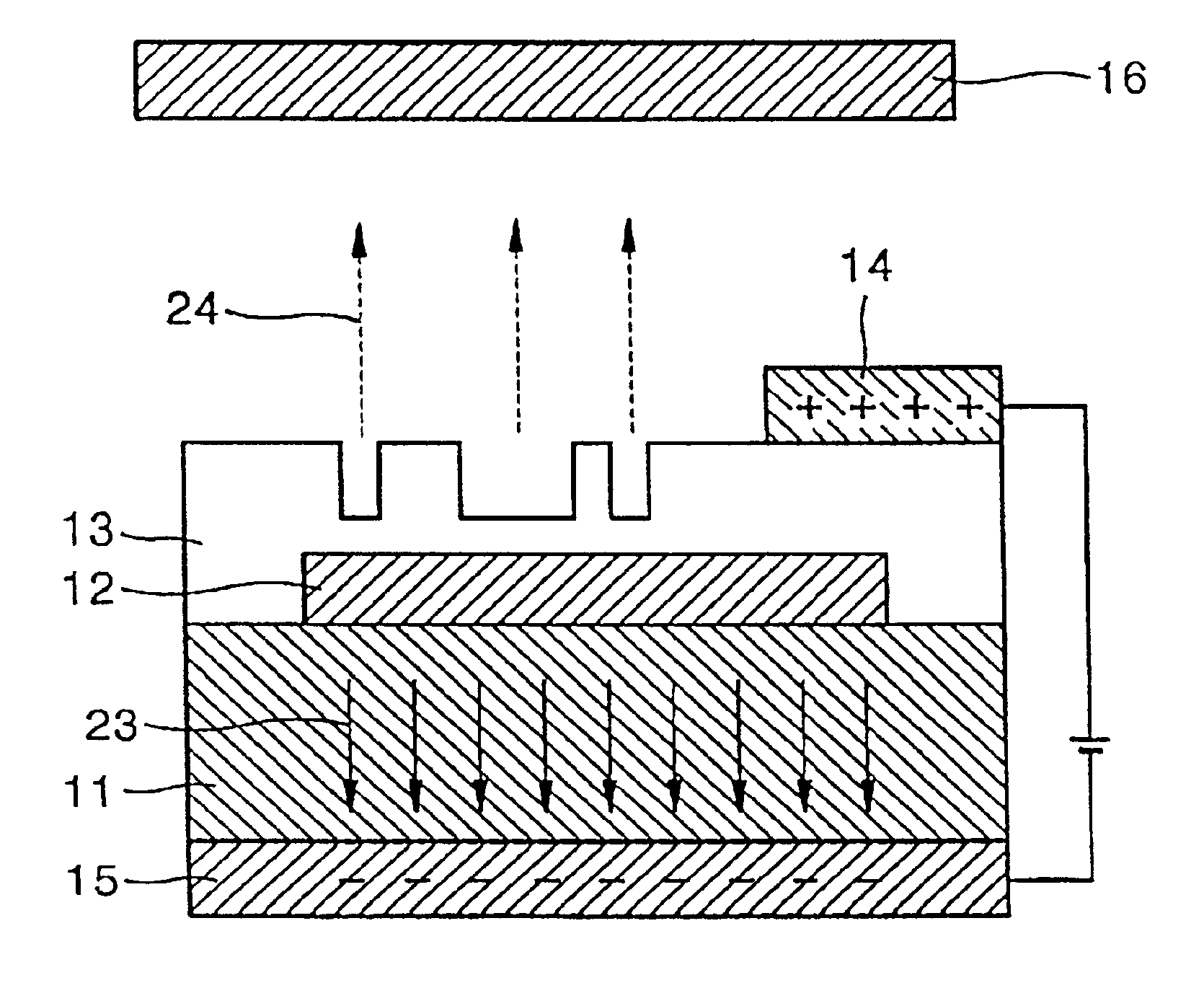
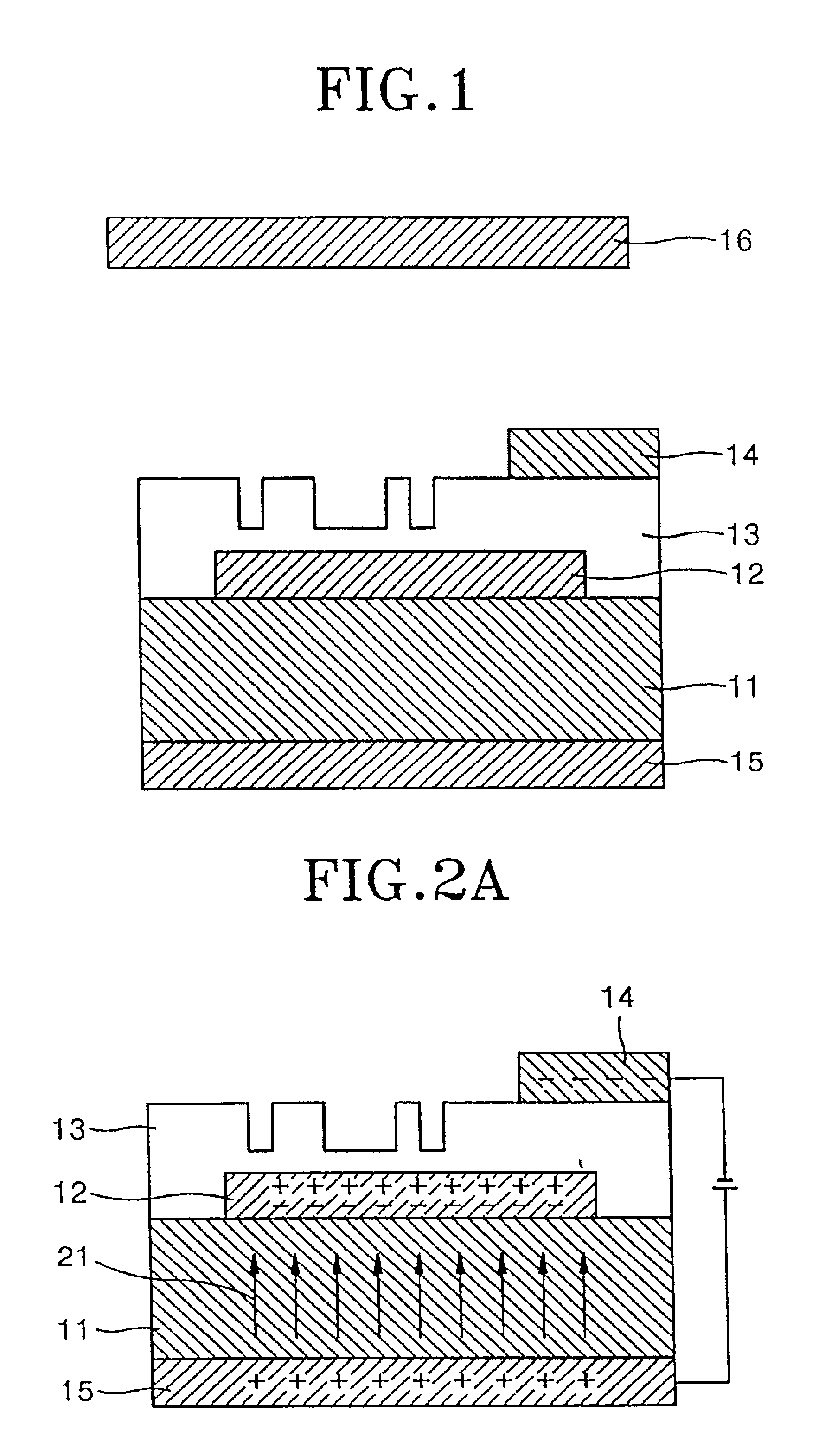
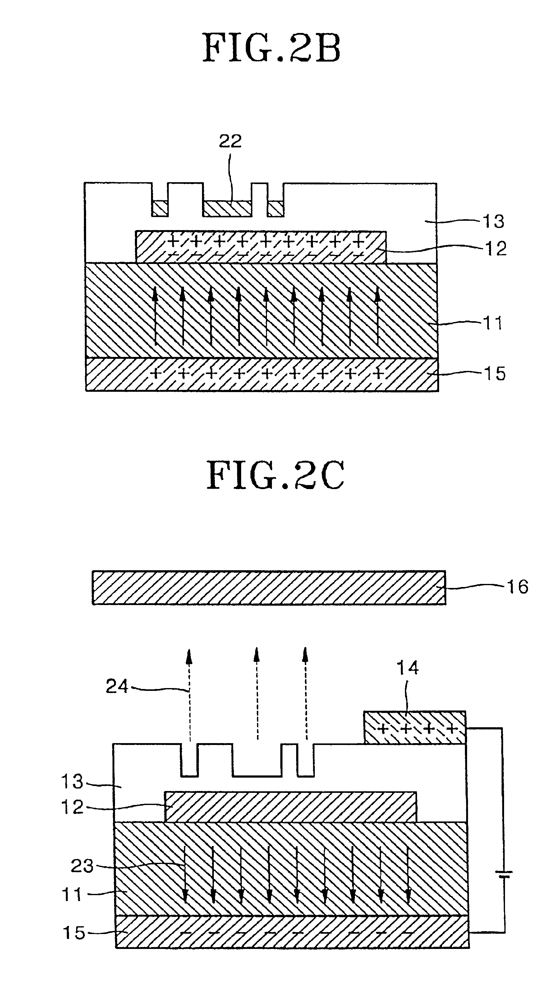
[0022]Referring to FIG. 1, a ferroelectric emitter according to a preferred embodiment of the present invention includes an insertion electrode 12 formed on a top surface of a ferroelectric layer 11. A dielectric layer 13 having a predetermined pattern is formed along the top surface of the ferroelectric layer 11 and the insertion electrode 12. The ferroelectric layer and the dielectric layer both having a top surface with two end portions. Thus, a top and two sides of the insertion electrode 12 are surrounded by the dielectric layer 13. Since the dielectric layer 13 is formed along the top surface of the ferroelectric layer 11 and the insertion electrode, a portion formed along the top surface of the ferroelectric layer 11 is thicker than a portion formed along a top surface of the insertion electrode 12. The predetermined pattern is formed at the top surface of the dielectric layer 13, over the insertion electrode 12.

[0023]A dummy upper electrode 14 is provided on the dielectric l...


PUM


Abstract

A ferroelectric multi-layered emitter used in a semiconductor lithography process includes a lower electrode, a ferroelectric layer, having a top surface with two end portions, which overlies the lower electrode, an insertion electrode formed on a region excluding the two end portions of the top surface of the ferroelectric layer, a dielectric layer, having sides and a top surface with two end portions, which has a predetermined pattern and is formed along the top surface of the ferroelectric layer and the insertion electrode, and a dummy upper electrode formed on a side of the dielectric layer opposite the ferroelectric layer. The ferroelectric emitter of the present invention guarantees uniform electron emission from wide and narrow gaps of a mask layer and in an isolated pattern such as a doughnut shape for ferroelectric switching emission lithography.

Description

BACKGROUND OF THF INVENTION[0001]1. Field of the Invention[0002]The present invention relates to a ferroelectric emitter. More specifically, the present invention relates to a ferroelectric multi-layered emitter used in a semiconductor lithography process.[0003]2. Description of the Related Art[0004]Ferroelectric emission by switching allows for a simple process in electron emission lithography. In the past, electron emission suitable for lithography has been obtained by switching an emitter in a magnetic field. However, a conventional ferroelectric emitter cannot guarantee electron emission where the gap between two electrodes is too wide or too narrow for switching.[0005]For example, in the conventional ferroelectric emitter, if the gap between two electrodes is too wide an electric field cannot reach the center portion of the ferroelectric emitter. Thus a switching effect does not occur in a ferroelectric region. If, on the other hand, the gap between the two electrodes, or a gap...

Claims


Application Information

Patent Timeline
IPC IPC(8): H01J37/06H01J1/30H01J37/073H01J1/312H01J37/04H01L21/027
CPCB82Y10/00B82Y40/00H01J37/073H01J37/3174H01J1/312H01J2201/306H01J1/30H01L21/027
Inventor YOO, IN-KYEONG
Owner SAMSUNG ELECTRONICS CO LTD
Why Eureka
Try Eureka