Method and system for displaying VLSI layout data

a layout design and layout technology, applied in the field of display of vlsi layout design, can solve the problems of inaccurate image, image not resembled to a photo, and process can take minutes to draw an entire image,

Inactive Publication Date: 2005-04-26
THE BOARD OF TRUSTEES OF THE LELAND STANFORD JUNIOR UNIV
View PDF4 Cites 29 Cited by
  • Summary
  • Abstract
  • Description
  • Claims
  • Application Information

AI Technical Summary

Benefits of technology

[0017]An object of the invention is to solve at least the above problems and/

Problems solved by technology

At magnification (or zoom), this process can take minutes to draw an entire image.
Additionally, since many of the features of the image are sub-pixel and/or fractional-pixel in dimension, the features appear incorrect, or “aliased” in the final image since the features will be drawn on pixel boundaries.
However, the image quality is decreased, and the image is inaccurate and does not resemble a photo-realistic image.
This method of culling speeds up the drawing process, but generates inaccuracies in the image.
However, the size of the image file created when the design is converted to an image could be terabytes, and consequently, the available techniques to view it as an image are limited.
However, using a clipmap or any other pur

Method used


Image

  • Method and system for displaying VLSI layout data
  • Method and system for displaying VLSI layout data
  • Method and system for displaying VLSI layout data

Examples


Embodiment Construction

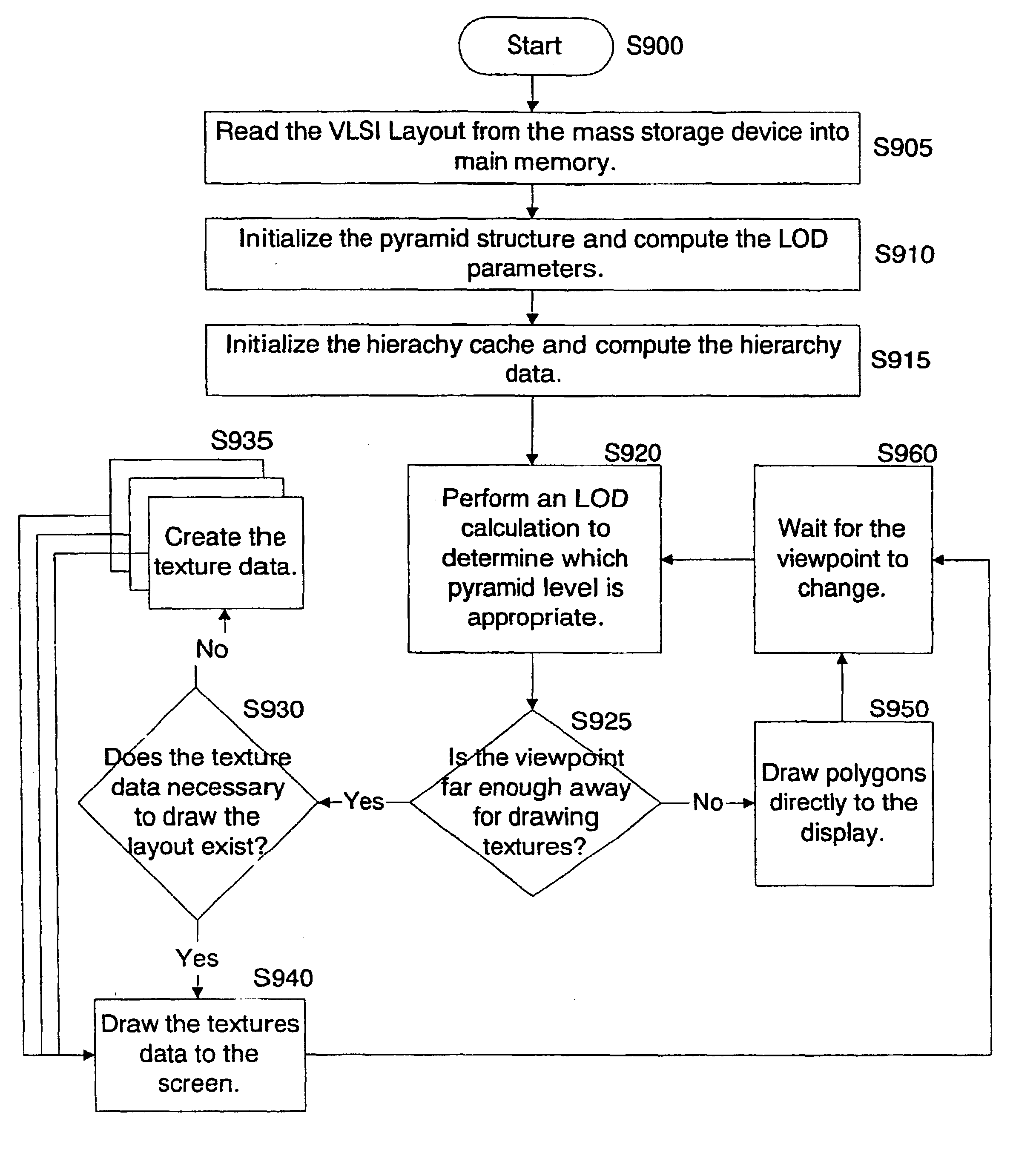
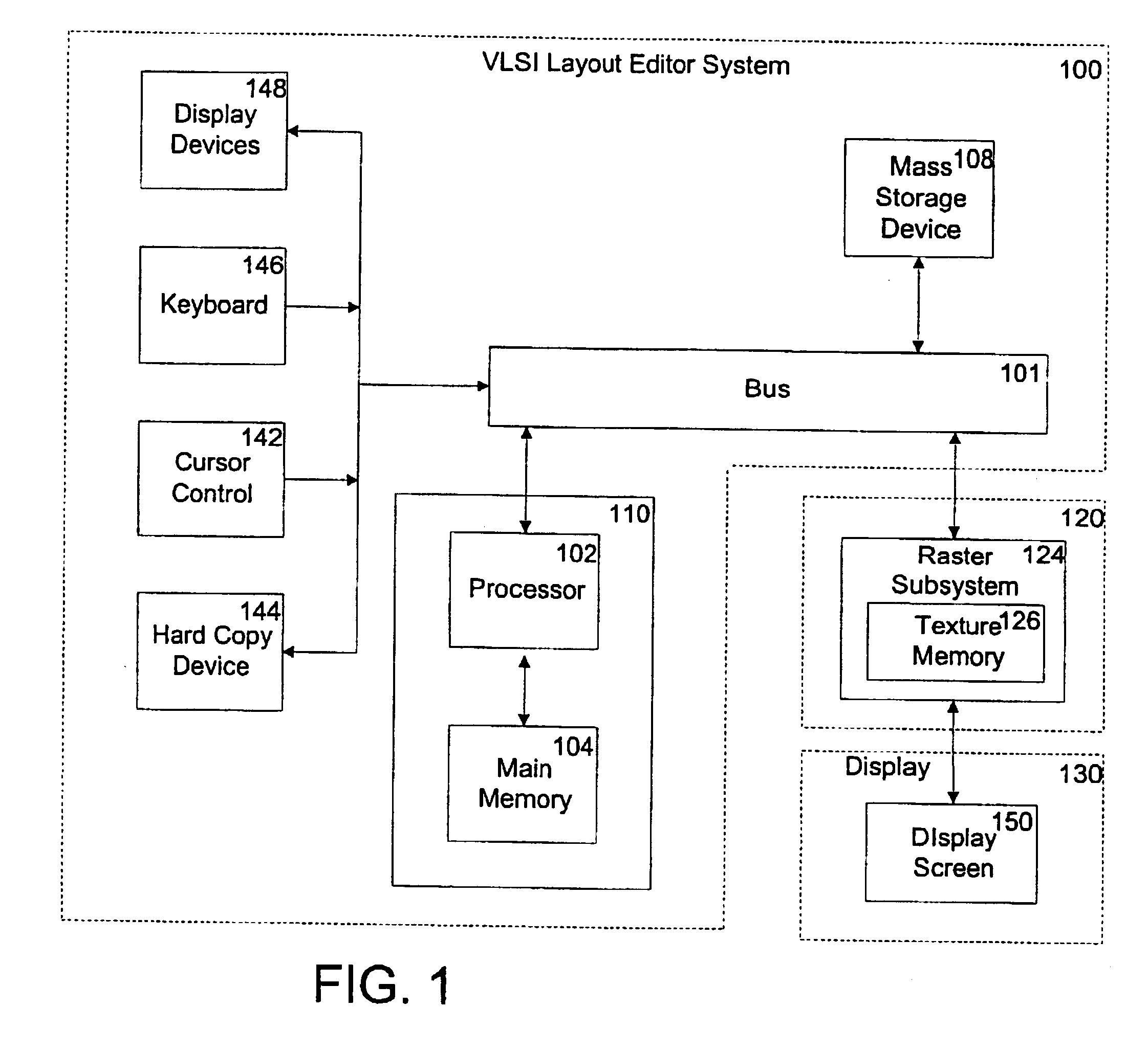
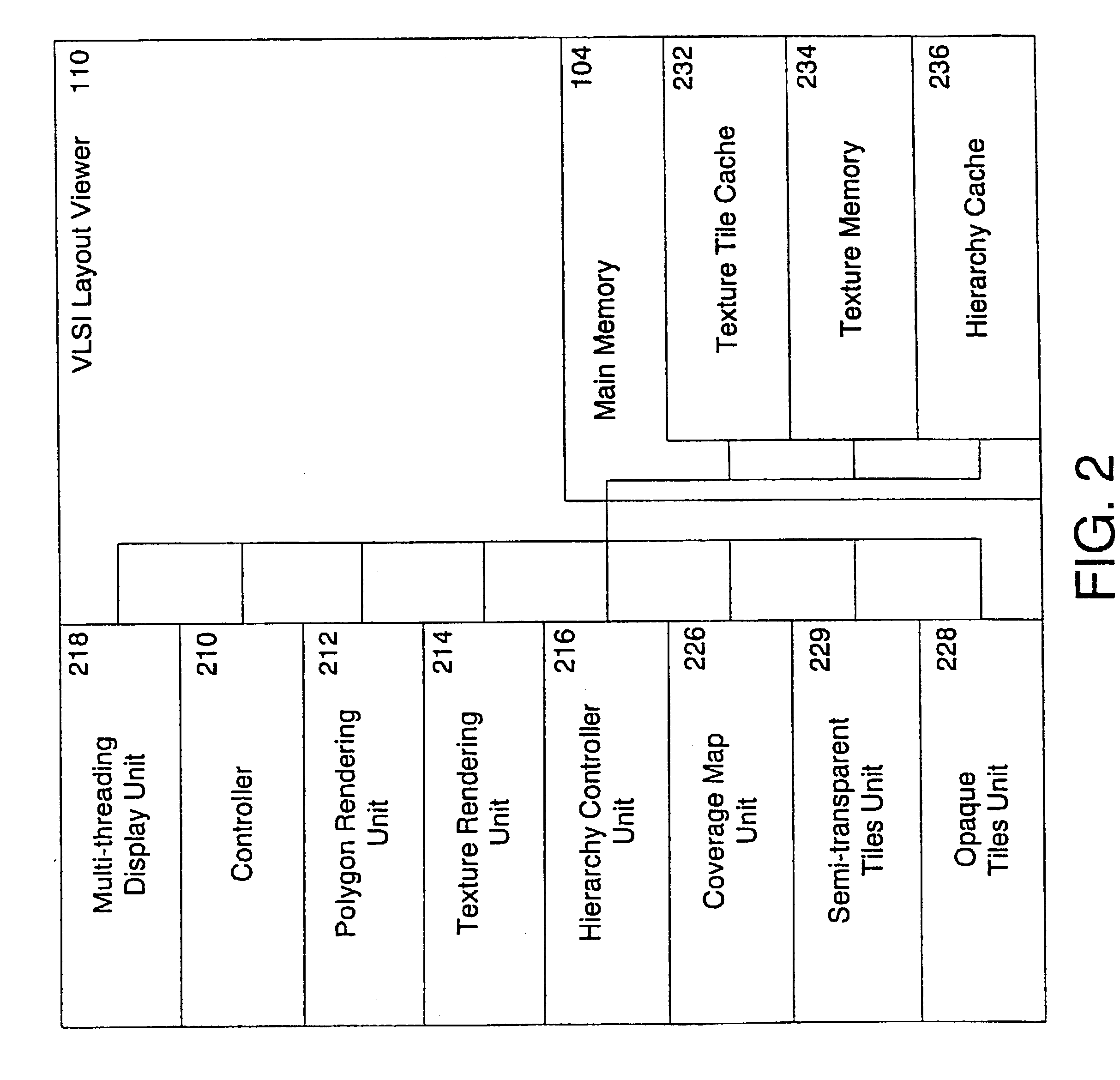
[0057]A preferred embodiment of a VLSI layout editor according to the present invention will now be described. FIG. 1 is a block diagram of a VLSI layout editor system 100 that includes a graphics subsystem 120 for generating display images for a display system 130 according to the present invention.

[0058]System 100 includes a mass storage device 108 and a VLSI layout viewer 110, which includes a host processor 102 and a main memory 104 coupled through a data bus 101. The mass storage device 108 is preferably used to store vast amounts of digital data. The mass storage device 108 initially stores one or more VLSI layouts in a canonical form. For example, the mass storage device 108 can include one or more hard disk drives, floppy disk drives, optical disk drives, tape drives, CD ROM drives, or any number of other types of storage devices having media for storing data digitally. For ease of description, this application will hereafter use the term VLSI layout viewer when describing v...


PUM


Abstract

A VLSI layout editor and method for using same that increases display and re-display speed and accuracy uses properties inherent to VLSI layouts that allows them to be displayed efficiently and accurately independent of the canonical expression of the VLSI design. The VLSI layout editor and methods for using same use precomputed images that each represent a portion of the VLSI layout, a hierarchy cache that includes multiple LOD versions of selected sub-designs in the pre-computed images, and selected direct determination of the viewable representation from the canonical expression for at least one LOD. Apparatus and methods according to the present invention can render a particular type of data whose canonical form is smaller than its corresponding displayed image thereof when the displayed image has geometric properties that allow heuristics and rasterization for dynamic and accurate expansion using selected combined techniques. Texture mapping and mipmapping can be used to accurately reduce, expand and reorder layers in a viewable image expanded from a canonical expression of the VLSI layout.

Description

[0001]This application is a Continuation of application Ser. No. 09 / 901,028 filed Jul. 10, 2001 (now U.S. Pat. No. 6,493,858), and claims priority to U.S. Provisional Application Ser. No. 60 / 278,001, filed Mar. 23, 2001, whose entire disclosure is incorporated herein by reference, and is subject to a contract made by Defense Advanced Research, Contract No. RFP-MOA904-98-R-5855.BACKGROUND OF THE INVENTION[0002]1. Field of the Invention[0003]Method and apparatus to display a VLSI layout design, and in particular, a CAD / CAM method and apparatus that displays a VLSI design in photo-realistic detail and in real-time.[0004]2. Background of the Related Art[0005]Computer systems are most always used for the display of data in VLSI designs. The amount of data to display can vary from design to design, and the largest designs can contain hundreds of millions of separate pieces of information. Manipulation of the design database is part of the design and manufacturing of VLSI chips. At some po...

Claims


Application Information

Patent Timeline
IPC IPC(8): G06F17/50G06T17/40G06T15/20G06T19/00
CPCG06F17/5068G06T15/20G06T19/00G06F30/39
Inventor SOLOMON, JEFFREY M.
Owner THE BOARD OF TRUSTEES OF THE LELAND STANFORD JUNIOR UNIV
Why Eureka
Try Eureka