Folding analog to digital converter capable of calibration and method thereof

an analog to digital converter and folding technology, applied in analogue/digital conversion, transmission systems, instruments, etc., can solve the problems of reducing the linearity of the adc, flash type adcs are undesirable for low power portable applications, and high power consumption of flash type adcs

Active Publication Date: 2005-05-03
REALTEK SEMICON CORP
View PDF4 Cites 69 Cited by
  • Summary
  • Abstract
  • Description
  • Claims
  • Application Information

AI Technical Summary

Benefits of technology

[0011]According to the claimed invention, an ADC is disclosed comprising at least one folder receiving an input voltage, generating a first output voltage and a second output voltage, and including a plurality of amplifiers and calibration logic for generating bias control signals according to the first output voltage and the second output voltage. Each of the amplifier receives one of a pl

Problems solved by technology

However, because the number of comparators grows exponentially with the resolution of the ADC, flash type ADCs have high power consumption and large integrated circuit (IC) chip area.
These characteristics make flash type ADCs undesirable for low power portable applications.
These imperfect characteristics of the amplifiers and pull-up resistors may reduce

Method used


Image

  • Folding analog to digital converter capable of calibration and method thereof
  • Folding analog to digital converter capable of calibration and method thereof
  • Folding analog to digital converter capable of calibration and method thereof

Examples


Embodiment Construction

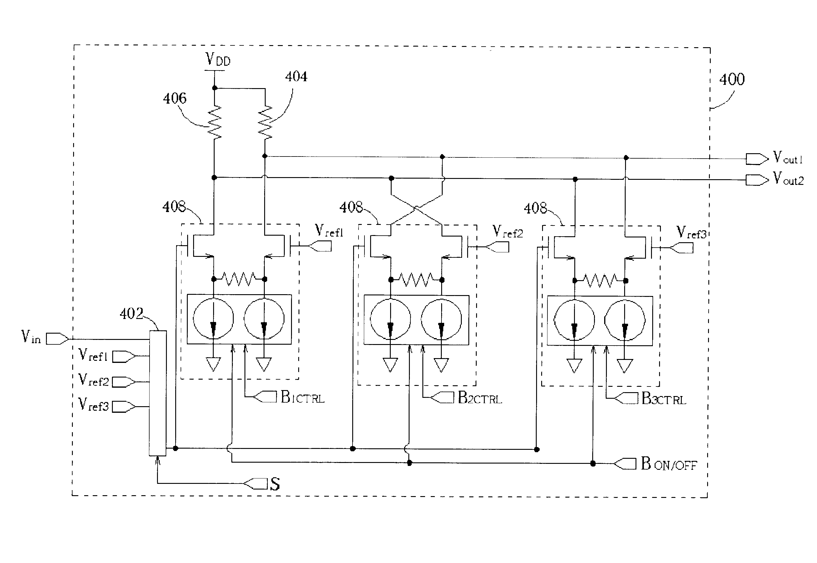
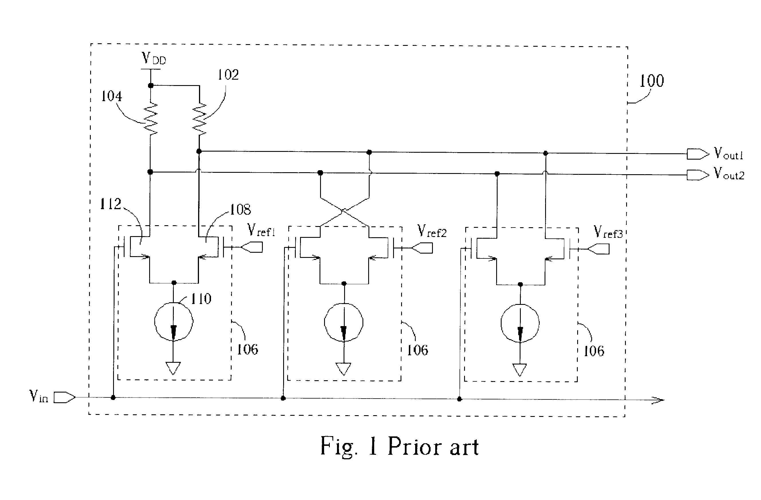
[0020]FIG. 3 shows a schematic diagram 300 of an amplifier 302 and calibration logic 304 according to an embodiment of the present invention. The amplifier 302 has a first input terminal for receiving a reference voltage Vref. A second input terminal of the amplifier 302 is connected to a switch 306, which is for selectively receiving either an input voltage Vin or the same reference voltage Vref. The amplifier 302 has a first output voltage Vout1 and a second output voltage Vout2, and the output voltages are pulled up to a power supply node VDD by a first pull-up resistor 308 and a second pull-up resistor 310, respectively. The amplifier 302 comprises a first transistor 312, a second transistor 314, an impedance 316, and a bias circuit 318.

[0021]The drains of the first transistor 312 and the second transistor 314 are for outputting the first and the second output voltage Vout1, Vout2, respectively. The gate of the first transistor 312 is for receiving the reference voltage Vref, an...


PUM


Abstract

An ADC is disclosed comprising at least one folder receiving an input voltage, generating a first output voltage and a second output voltage, and including a plurality of amplifiers and calibration logic for generating bias control signals according to the first output voltage and the second output voltage. Each of the amplifier receives one of a plurality of reference voltages and comprises a bias circuit for providing a bias current to the amplifier based on at least one of a plurality of bias control signals. During calibration, the calibration logic provides the bias control signals to control the bias circuit of each amplifier in the folder such that the first output voltage is substantially the same as the second output voltage.

Description

BACKGROUND OF INVENTION[0001]1. Field of the Invention[0002]The invention relates to an analog to digital converter, and more particularly, to a folding analog to digital converter capable of calibration and method thereof.[0003]2. Description of the Prior Art[0004]Analog to digital converters (ADCs) allow the use of sophisticated digital signal processing systems to process analog signals, which are common in the real world. High-speed ADCs are critical components of digital signal processing systems.[0005]Flash type ADCs are commonly used for high speed signal applications. In a flash type ADC, a separate comparator is used for each possible output code bit, and this parallelism is what gives the flash ADC its speed. However, because the number of comparators grows exponentially with the resolution of the ADC, flash type ADCs have high power consumption and large integrated circuit (IC) chip area. These characteristics make flash type ADCs undesirable for low power portable applic...

Claims


Application Information

Patent Timeline
IPC IPC(8): H03M1/14H03M1/36H03M1/10H03M1/16H03M1/12
CPCH03M1/1014H03M1/141
Inventor HERTLE, FRITZ JUERGEN
Owner REALTEK SEMICON CORP
Why Eureka
Try Eureka