Microelectromechanical switch (MEMS) antenna array

a micro-electromechanical switch and antenna array technology, applied in the direction of antennas, antenna details, antenna feed intermediates, etc., can solve the problems of affecting the performance of each antenna, and difficulty in housing a corresponding plurality of microstrip antennas

Inactive Publication Date: 2005-05-03
KYOCERA CORP
View PDF3 Cites 20 Cited by
  • Summary
  • Abstract
  • Description
  • Claims
  • Application Information

AI Technical Summary

Benefits of technology

[0013]The present invention provides a microstrip, or printed circuitboard antenna that is made with MEMSs to vary the actual physical length of the printed line active element radiators. The MEMSs can be used to form selectable connected conductive sections that vary the length of the antenna active element, thereby changing t

Problems solved by technology

As a result, the designers must increase the performance of components or device subsystems while reducing their size, or placing these components in less desirable locations.
However, a wireless device that is expected to operate at a plurality of different frequencies may have difficulty housing a corresponding plurality of microstrip antennas.
Even if all

Method used


Image

  • Microelectromechanical switch (MEMS) antenna array
  • Microelectromechanical switch (MEMS) antenna array
  • Microelectromechanical switch (MEMS) antenna array

Examples


Embodiment Construction

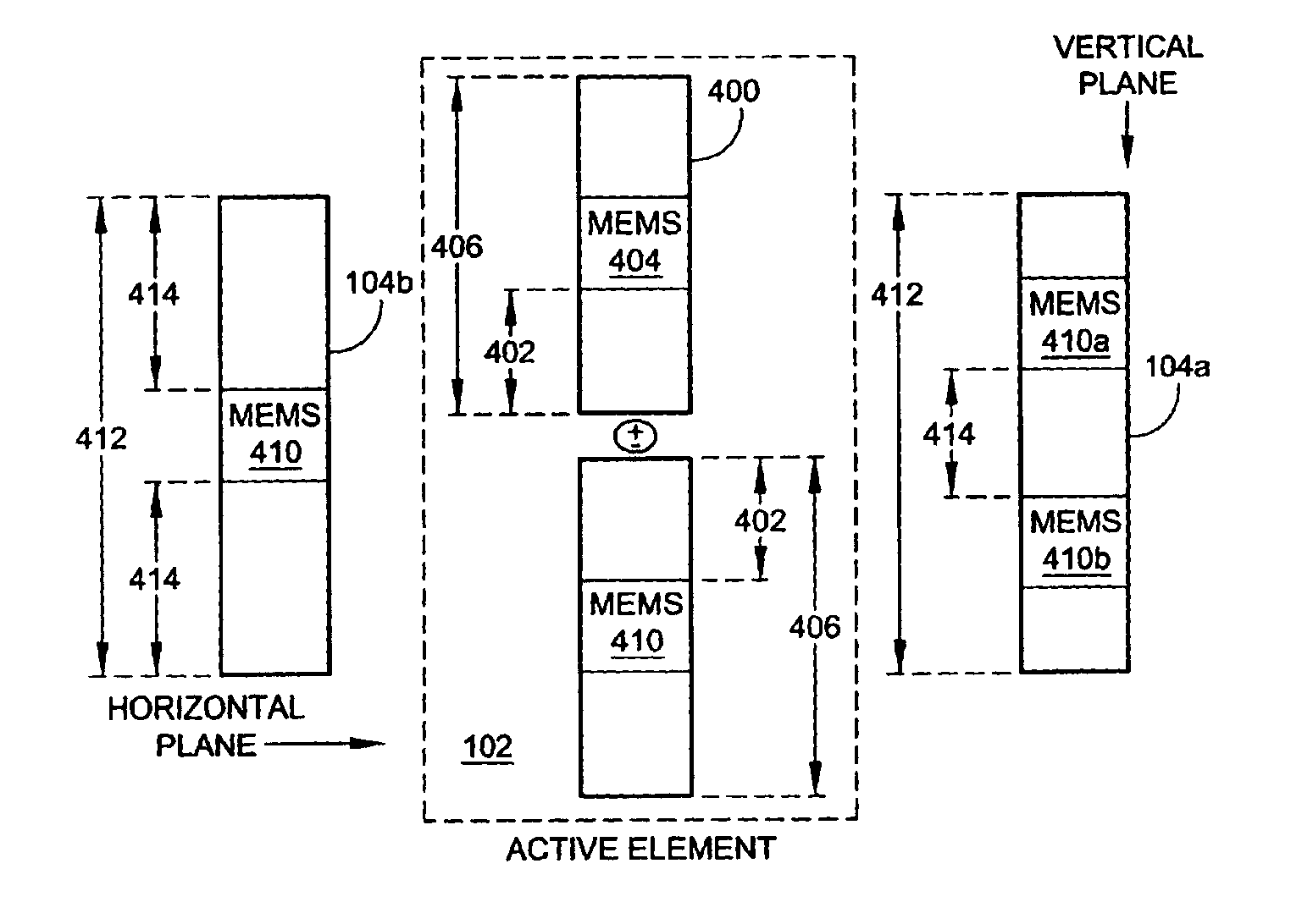
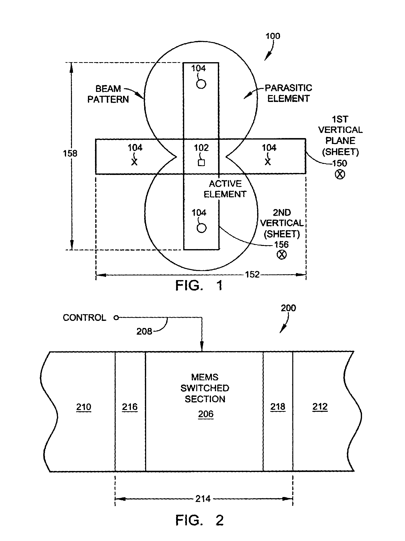
[0038]FIG. 1 is a plan view of the present invention microelectromechanical switch (MEMS) beam-steering antenna array. The antenna array 100 comprises an active element 102 including a selectively connectable MEMS and a lattice of beam-forming parasitic elements 104. Each parasitic element includes a selectively connectable MEMS, proximate to the active element 102. The “X” pattern indicates an engaged parasitic element 104 and an “O” pattern represents a disengaged parasitic element 104. FIG. 1 depicts one possible parasitic element lattice and the resulting antenna pattern.

[0039]As shown in the partially cross-sectional view of FIG. 18, each MEMS 200 includes a dielectric layer 202 and a conductive line 204, with a selectively connectable MEMS conductive section 206, formed overlying the dielectric layer.

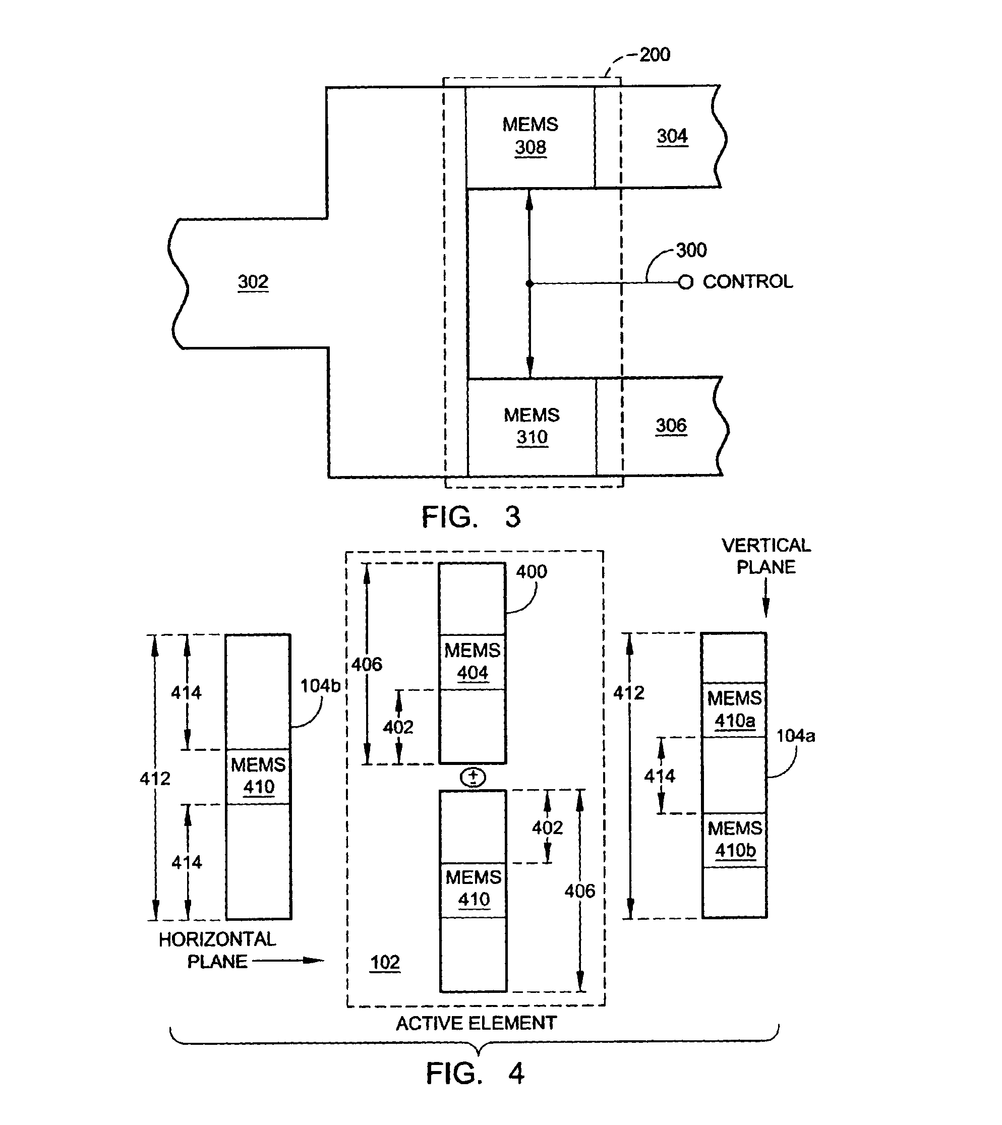
[0040]FIG. 2 is a more detailed plan depiction of a MEMS device 200, suitable for use in either an active element or a parasitic element. The MEMS 200 has a control input on line ...


PUM


Abstract

A microelectromechanical switch (MEMS) beam-steering antenna array is provided. The antenna comprises an active element including a selectively connectable MEMS, and a lattice of beam-forming parasitic elements, each including a selectively connectable MEMS, proximate to the active element. In some aspects, the active element is a dipole radiator having an effective quarter-wavelength odd multiple length at a first plurality of frequencies in response to connecting radiator MEMS. Likewise, the dipole counterpoise has an effective quarter-wavelength odd multiple length at the first plurality of frequencies in response to connecting counterpoise MEMS. Further, each parasitic element has an effective half-wavelength odd multiple length at the first plurality of frequencies in response to connecting their corresponding MEMS. In other aspects, the active element is a monopole and includes a radiator with a radiator MEMS, a counterpoise groundplane, and parasitic elements with MEMSs.

Description

BACKGROUND OF THE INVENTION[0001]1. Field of the Invention[0002]This invention generally relates to wireless communications antennas and, more particularly, to a selectable antenna array formed from a microelectromechanical switch.[0003]2. Description of the Related Art[0004]The size of portable wireless communications devices, such as telephones, continues to shrink, even as more functionality is added. As a result, the designers must increase the performance of components or device subsystems while reducing their size, or placing these components in less desirable locations. One such critical component is the wireless communications antenna. This antenna may be connected to a telephone transceiver, for example, or a global positioning system (GPS) receiver.[0005]Wireless telephones can operate in a number of different frequency bands. In the US, the cellular band (AMPS), at around 850 megahertz (MHz), and the PCS (Personal Communication System) band, at around 1900 MHz, are used. ...

Claims


Application Information

Patent Timeline
IPC IPC(8): H01Q9/04H01Q9/28H01Q3/24
CPCH01Q3/24H01Q9/28H01Q3/247
Inventor TRAN, ALLEN
Owner KYOCERA CORP
Why Eureka
Try Eureka