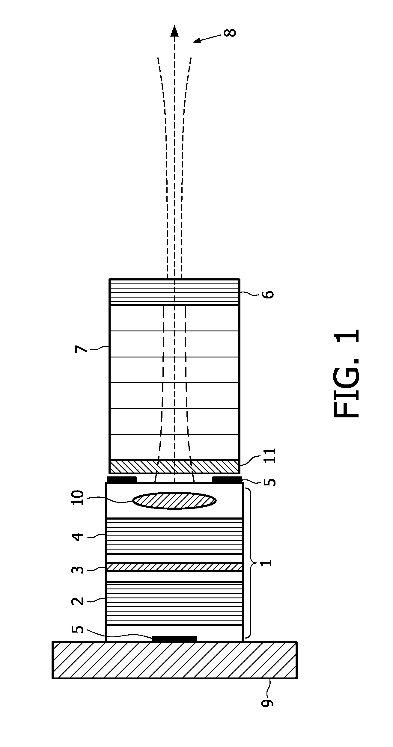
[0007]It is an object of the present invention to provide a semiconductor laser device, in particular a VECSEL device, generating high power fundamental laser radiation with significantly reduced spectral bandwidth.
[0011]The invention is based on the coherent coupling of
laser beams of several VECSELs via constructive interference. The beams of the different VECSEL components are overlaid via the coupling component which acts like an interferometric beam combiner. The beam combiner preferably provides one or several
beam splitting regions for appropriately combining the different
laser beams to one single laser beam. At such a
beam splitting region, for example when combining two
laser beams, a portion of one of the laser beams is reflected or transmitted outside of the extended cavity. Since the laser will always tend to operate in a mode which minimizes losses, the interference between both laser beams will adjust in such a way, that the beams in the loss channel will interfere destructively, while the beams in the extended cavity will interfere constructively. Therefore, even though in principle substantial losses would be expected in such a type of cavity, the losses are avoided by destructive interference and the two laser beams are constructively added resulting in a coherent emission of both beams. The same applies to the coupling of more than two laser beams when using an array of more than two VECSEL components. Due to this coherent coupling a significant spectral narrowing is achieved, since all coupled lasers have to share a common longitudinal cavity mode while operating in laser resonators of different length. The same argument also holds true for the transverse
modes. Therefore the coherent coupling of the different VECSEL components also results in a substantial improvement of the beam quality. The output of the proposed VECSEL device is correspondingly increased with the number of VECSEL components included in the device. Due to the significant spectral narrowing, the improved beam quality and the higher intensity of the fundamental radiation, preferably infrared radiation, the proposed laser device can be very advantageously used for intracavity or extra cavity frequency conversion, in particular when using frequency converting crystals as for example crystals for second harmonic generation.
[0012]Due to the spectral narrowing of the coherently coupled laser beams, there is no need for any additional spectral selectivity inside of the cavity. Therefore, much simpler outcoupling mirrors than volume Bragg gratings can be employed. For example, cheap
broadband dielectric mirrors can be used for outcoupling, or a
dielectric coating can be directly applied to the
exit surface of the
optical coupling component, in which the laser beams are coupled. The proposed laser device allows a very compact construction for generating the desired laser radiation.
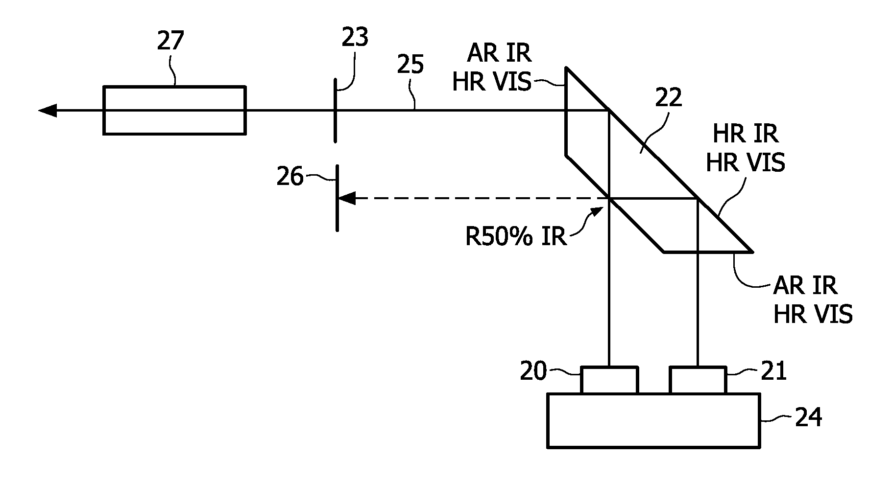
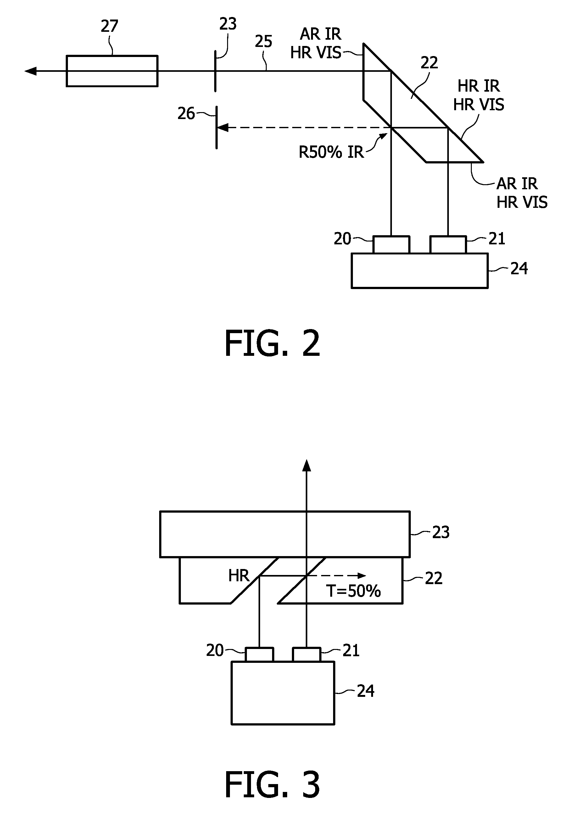
[0016]The coupling component preferably comprises two opposing
reflective surfaces for
beam coupling. One of these surfaces is highly reflective (
reflectivity≧95%) for the fundamental laser radiation, whereas the other surface has a
reflectivity of between 40 and 60%, preferably 50%, and a
transmittance of between 40 and 60%, preferably 50%, for the fundamental laser radiation. With such a coupling component a large number of laser beams can be combined using multiple internal reflections between the two opposing surfaces. In one advantageous embodiment, in which frequency upconversion is performed outside of the extended cavities, the coupling component is directly attached to the second end mirror, i.e. the outcoupling mirror for the fundamental radiation, or this mirror is formed by an appropriate
coating on an outcoupling surface of the coupling component. This results in a very compact construction of the whole device.
[0017]In a further advantageous embodiment, the second end mirror is attached to a translation stage with which the second end mirror may be displaced to vary the length of the extended cavities. Such a translation stage may be formed of an appropriate
actuator, for example a piezo-
actuator. When using an
optical detector measuring the intensity of outcoupled laser radiation, the length of the laser cavities can be varied through an appropriate
control unit based on the measured intensity. With such an arrangement, the operation of the laser device can be optimized to have desired properties, for example a maximum output intensity and / or a stable operation. This allows for compensating any cavity length detuning, which can appear for example when the temperature of the laser device varies during operation and the
optical path lengths of the external cavities change due to the resulting
refractive index changes within the semiconductor material.
[0018]When using the proposed laser device with a frequency converting medium,
green laser radiation can be generated with high power. Therefore, such a device can advantageously be used as one of the components of a RGB
laser source or as one of the light sources in a
laser projection device.

