Sensor for performing surface enhanced Raman spectroscopy and method for achieving same

a raman spectroscopy and sensor technology, applied in the field of raman spectroscopy, can solve the problems of raman scattering, surface enhanced raman spectroscopy (sers), insensitive technique, etc., and achieve the effects of enhancing raman scattering, enhancing raman scattering, and minimizing the effect of raman scattering

Inactive Publication Date: 2005-05-03
THE UNITED STATES OF AMERICA AS REPRESENTED BY THE SECRETARY OF THE NAVY
View PDF14 Cites 21 Cited by
  • Summary
  • Abstract
  • Description
  • Claims
  • Application Information

AI Technical Summary

Benefits of technology

[0009]A sensor performs surface enhanced Raman spectroscopy and employs a filter to minimize the effects of Raman scattering to self-excitation of the optical elements of the sensor. The sensor comprises: a) a sensor body having a throughbore; an optical energy source for generating an optical excitation signal; b) a surface enhanced Raman scattering structure that is mounted to the sensor body through which the optical excitation signal is directed for irradiating an analyte, whereupon the analyte generates primary Raman emissions in response to being irradi

Problems solved by technology

Despite the advantages of Raman spectroscopy over other spectroscopic techniques and the technological advances in the area of Raman spectrometry, Raman spectroscopy is, inherently, an insensitive technique.
This phenomenon, called surface enhanced Raman spectroscopy (SERS), is

Method used


Image

  • Sensor for performing surface enhanced Raman spectroscopy and method for achieving same
  • Sensor for performing surface enhanced Raman spectroscopy and method for achieving same
  • Sensor for performing surface enhanced Raman spectroscopy and method for achieving same

Examples


Embodiment Construction

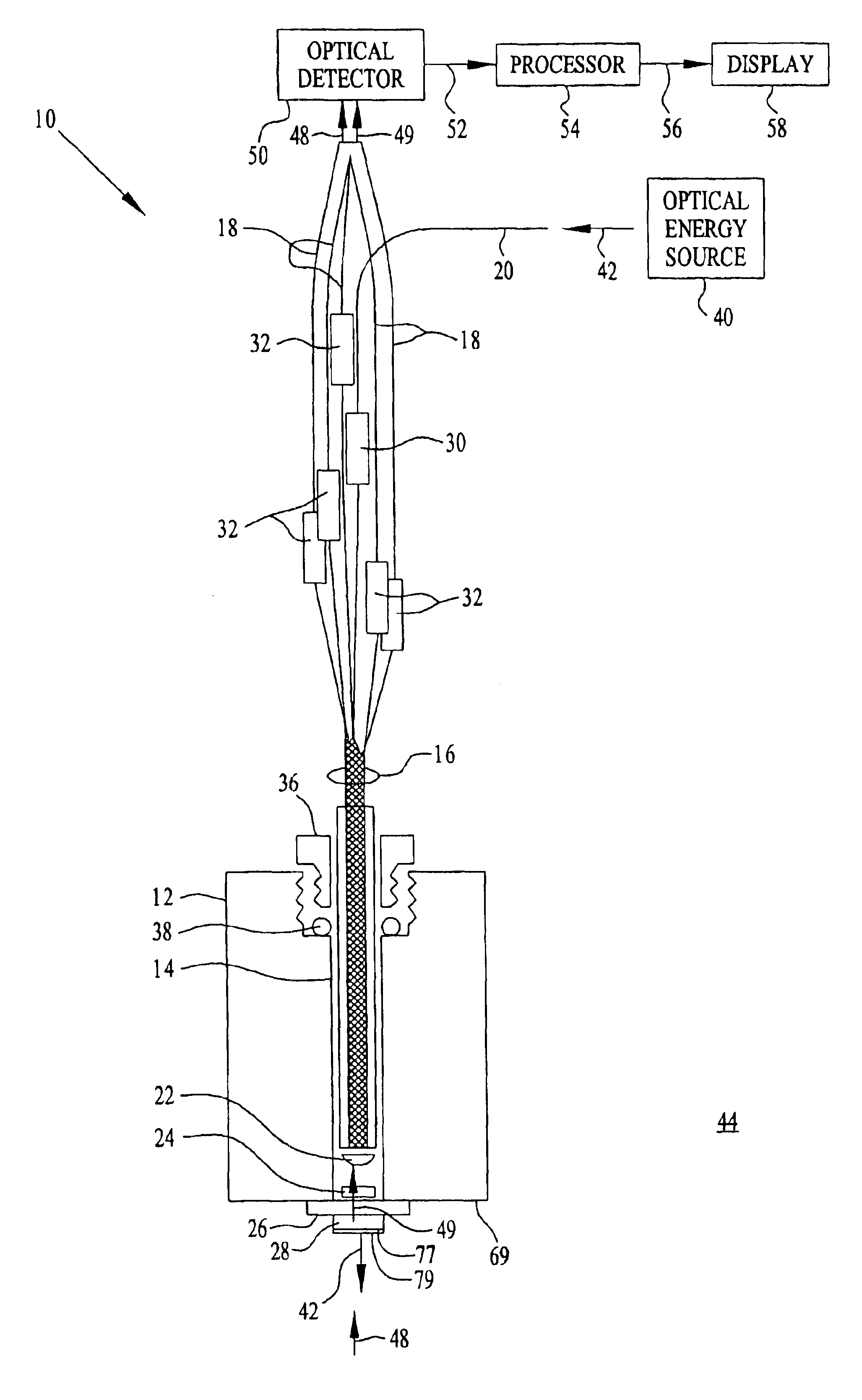
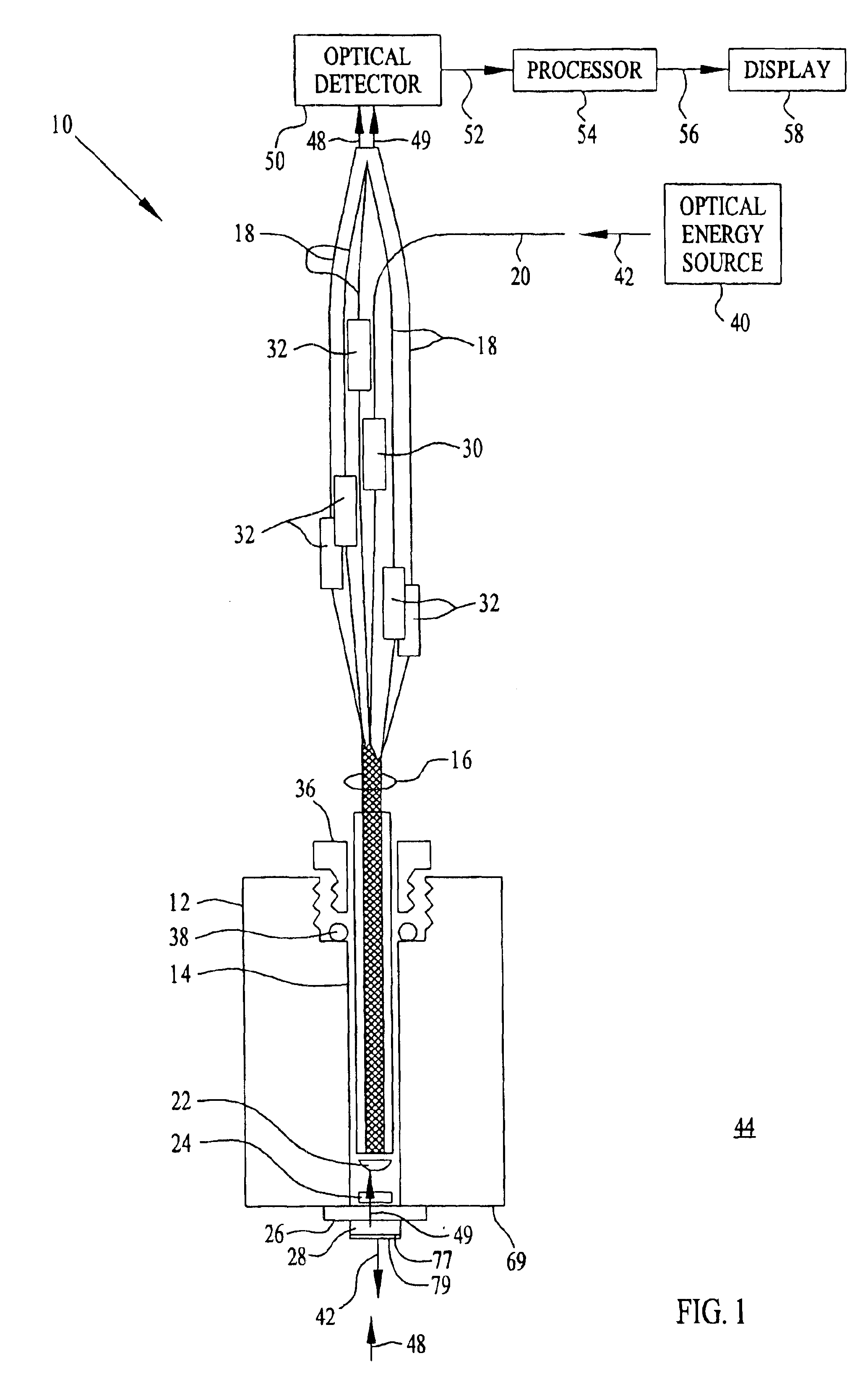
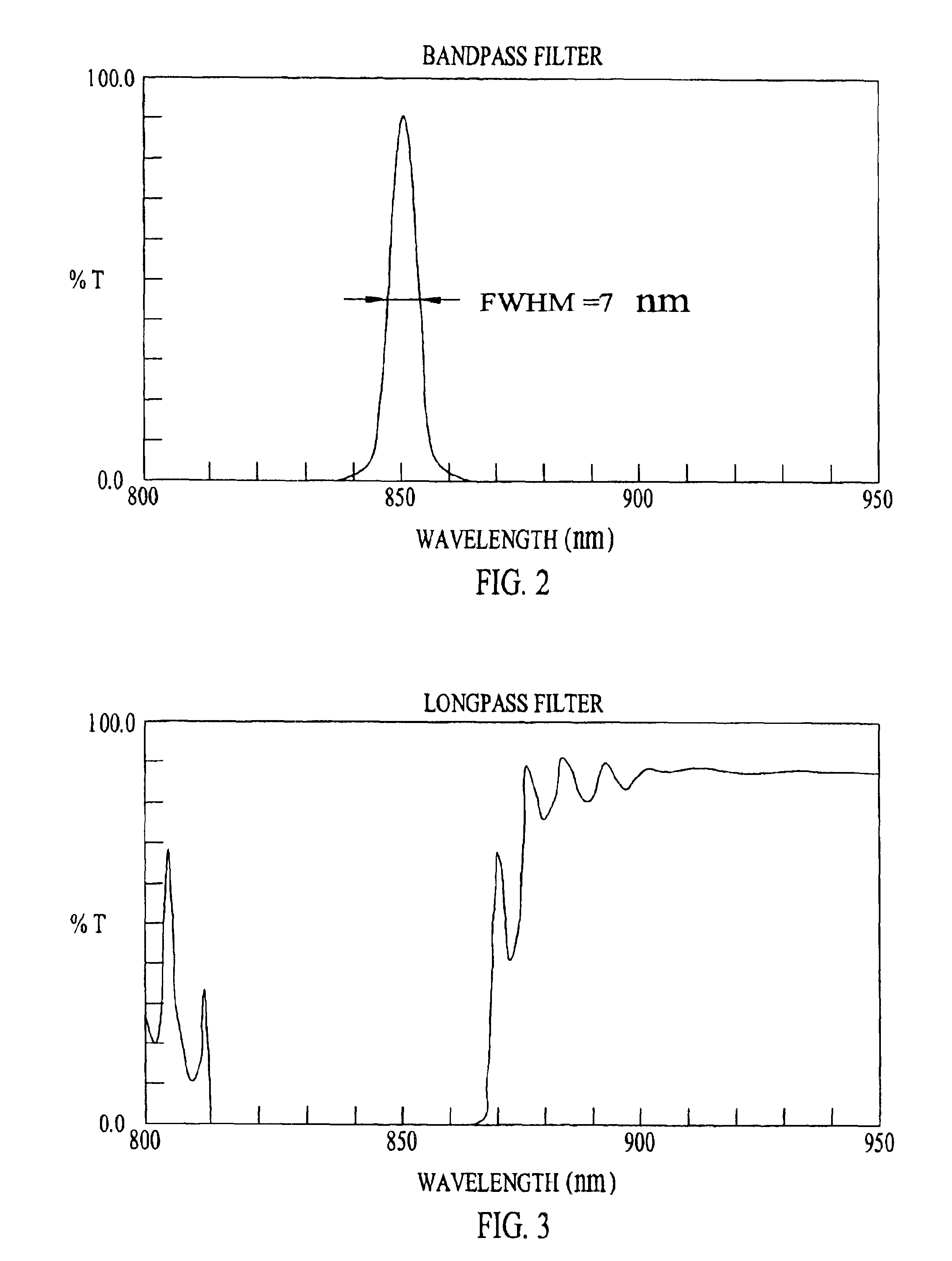
[0015]Referring to FIG. 1, the present invention is directed to a sensor 10 for performing surface enhanced Raman spectroscopy. The sensor 10 includes a sensor body 12 having a throughbore 14 in which is positioned a fiber optic bundle 16 comprised of collection optical fibers 18, excitation optical fiber 20, collimating lens 22, focusing lens 24, window 26, and a Surface Enhanced Raman Spectroscopy (SERS) structure 28 that is described in commonly assigned U.S. patent application Ser. No. 09 / 593,675, filed 14 Jun. 2000, and entitled A METAL AND GLASS STRUCTURE FOR USE IN SURFACE ENHANCED RAMAN SPECTROSCOPY AND METHOD FOR FABRICATING SAME, incorporated herein by reference. Filter 30 is optically aligned and spliced to excitation optical fiber 20; and an optical filter 32 is optically aligned and spliced to each of collection optical fibers 18. Bushing 36 is threaded into sensor body 12 to secure the fiber optic bundle 16 within the bore 14 of the sensor body 12. An O-ring 38 may be ...


PUM

PropertyMeasurementUnit
Wavelengthaaaaaaaaaa
Optical propertiesaaaaaaaaaa

Abstract

A sensor for performing surface enhanced Raman spectroscopy comprises: a) a sensor body having a throughbore; an optical energy source for generating an optical excitation signal; b) a surface enhanced Raman scattering structure that is mounted to the sensor body through which the optical excitation signal is directed for irradiating an analyte, whereupon the analyte generates primary Raman emissions in response to being irradiated by the optical excitation signal, and wherein the surface enhanced Raman scattering structure generates secondary Raman emissions when irradiated by the optical excitation signal; c) an optical detector for generating an output signal that represents the spectral characteristics of the primary and secondary Raman emissions in response to receiving the primary and second Raman emissions; and d) a processor for substantially filtering the secondary Raman emission from the primary Raman emissions and for generating an output signal representing the analyte.

Description

CROSS REFERENCE TO RELATED APPLICATIONS[0001]This application is a continuation-in-part of commonly assigned U.S. patent application Ser. No. 09 / 593,675, filed 14 Jun. 2000, now U.S. Pat. No. 6,406,777 and entitled A METAL AND GLASS STRUCTURE FOR USE IN SURFACE ENHANCED RAMAN SPECTROSCOPY AND METHOD FOR FABRICATING SAME, and is a continuation-in-part of commonly assigned U.S. patent application Ser. No. 09 / 805,665, filed 13 Mar. 2001, now U.S. Pat. No. 6,614,523 and entitled SENSOR FOR PERFORMING SURFACE ENHANCED RAMAN SPECTROSCOPY.BACKGROUND OF THE INVENTION[0002]The present invention generally relates to the field of Raman spectroscopy, and more particularly, to a sensor for detecting chemicals both in gas and liquid environments using surface enhanced Raman spectroscopy in which any Raman scattering due to excitation of the optical elements of the sensor are minimized.[0003]Raman spectroscopy is an emission technique that involves inelastic scattering of incident laser energy and...

Claims


Application Information

Patent Timeline
IPC IPC(8): C03C17/36C03C17/38G01N33/551G01N33/543G01N33/552G01N21/65
CPCB82Y15/00B82Y30/00C03C17/38G01N33/552G01N21/658G01N33/54373C03C2217/77C03C2204/08G01N21/8507
Inventor BOSS, PAMELA A.LIEBERMAN, STEPHEN H.
Owner THE UNITED STATES OF AMERICA AS REPRESENTED BY THE SECRETARY OF THE NAVY
Why Eureka
Try Eureka