
System and method for fingerprinting of semiconductor processing tools

Active Publication Date: 2005-05-03
ASM INTERNATIONAL
View PDF11 Cites 2 Cited by
  • Summary
  • Abstract
  • Description
  • Claims
  • Application Information

AI Technical Summary

Benefits of technology

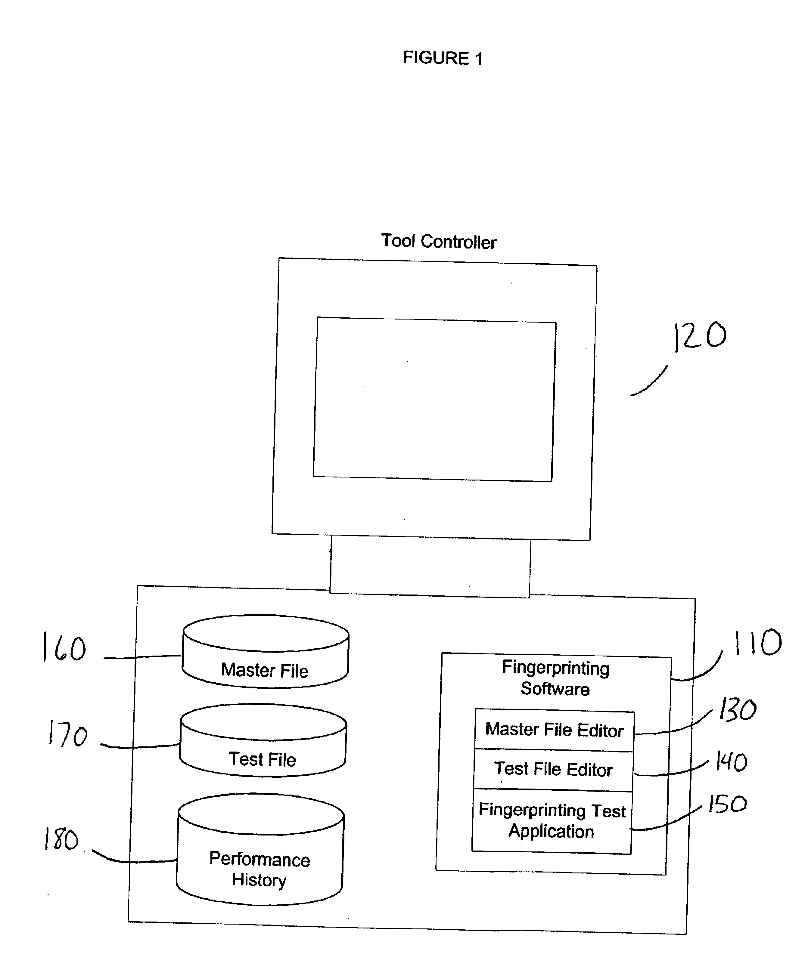
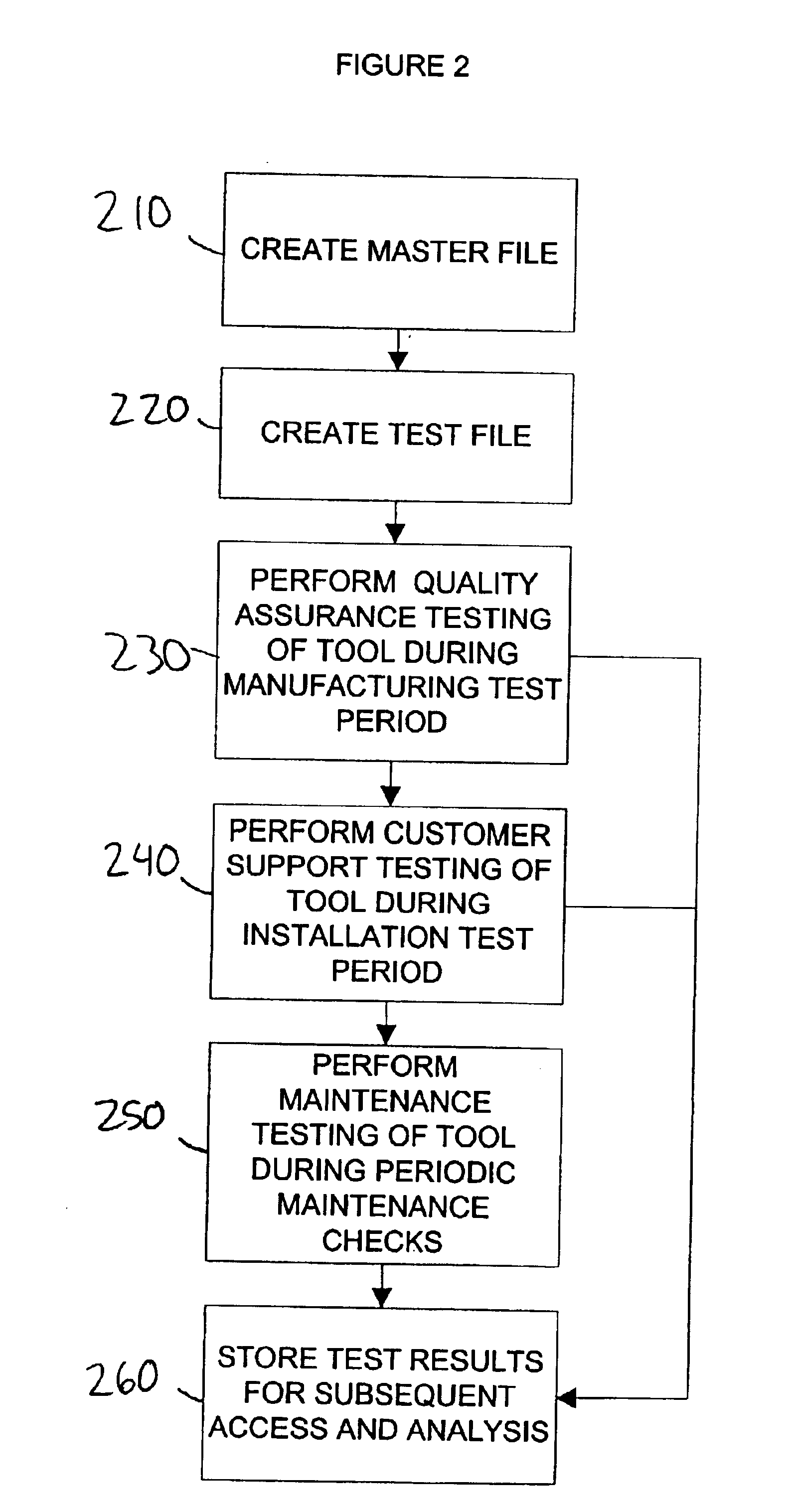
[0007]Therefore, a need exists for a system and method that performs one or more of the following functions: conveniently collects and stores measured values of tool parameters of a semiconductor processing tool in a quality assurance procedure during manufacturing of the tool, verifies automatically if the values of the measured parameters are within predefined limits, provides an indication relating to the status and value of the measured parameters, and allows end users of a processing tool to repeat the test and compare the test results with the results of previous tests.

Problems solved by technology

Typically, the quality assurance steps described herein are not performed during wafer processing; accordingly, the processing tool is typically void of actual production wafers during quality assurance testing as described herein.

Method used


Image

  • System and method for fingerprinting of semiconductor processing tools
  • System and method for fingerprinting of semiconductor processing tools
  • System and method for fingerprinting of semiconductor processing tools

Examples


Embodiment Construction

[0030]To facilitate a complete understanding of the invention, the remainder of the detailed description describes the invention with reference to the drawings.

[0031]With reference to FIGS. 16 and 17, an exemplary semiconductor processing system containing a process chamber is illustrated and indicated generally by the reference numeral 30. The exemplary system 30 of FIGS. 16 and 17 comprises a housing 32 and is generally installed in a so-called “clean room.” In addition to the housing 32, partitions 33, 34 and 35 (omitted from FIG. 16 for clarity of illustration) are also present. The housing 32 delimits, with the partition 33, a processing chamber 51. The processing area 51 comprises reactors, which in this example, are vertical furnaces 36, 37. The housing 32 and the partitions 33 and 34 define a wafer handling section or chamber 52. A cassette transfer section or chamber 53 is defined between the housing 32 and partitions 34 and 35. An input / output station, to transfer cassette...


PUM


Abstract

A system and method is used for measuring the performance of semiconductor processing tools. A software component may be used to define a set of performance variables and associate performance limits. From the set of performance variables, a set of variables may be selected to create a customized test for a particular tool. The system may be used to store the results of the tests within the system for fast comparison with the associated performance limits, with previous test results, or both. The system may be used to display an overall status of groups of performance variables.

Description

FIELD OF THE INVENTION[0001]The invention relates to the field of processing equipment and more particularly to quality control testing of such equipment.BACKGROUND OF THE INVENTION[0002]In manufacturing products, a processing tool executes a treatment according to predetermined conditions on material to be treated. Examples are semiconductor processing tools for the treatment of semiconductor wafers, chemical reactors etc. A semiconductor processing tool typically comprises a number of devices like wafer-handling robots, valves, mass flow controllers, a temperature controller providing input signals to a thyristor pack or silicon controlled rectifier, empowering a heating element, etc. A semiconductor processing tool controller controls these devices to effectuate control over processing conditions such as gas flows, pressure, temperature, etc. For this purpose, the controller comprises a number of digital inputs and outputs and a number of analog inputs and outputs. Via the output...

Claims


Application Information

Patent Timeline
IPC IPC(8): H01L21/00G05B23/02
CPCG05B23/0256G05B23/0264H01L21/67276
Inventor SIEGERS, JOHANHAANSTRA, KORNELIUSZINGER, JAN
Owner ASM INTERNATIONAL
Learn More