Circuitry and methodology to establish correlation between gate dielectric test site reliability and product gate reliability

a gate dielectric test site and reliability technology, applied in the field of reliability testing of integrated circuits, can solve the problems of product samples being subjected, and the correlation to the reliability of produce seems to become more elusiv

Inactive Publication Date: 2005-05-10
IBM CORP
View PDF3 Cites 2 Cited by
  • Summary
  • Abstract
  • Description
  • Claims
  • Application Information

AI Technical Summary

Benefits of technology

[0006]An object of this invention is to provide an improved method and system to establish the correlation between gate dielectric test site reliability and product gate reliability.

Problems solved by technology

To accomplish this in a short time, product samples may be subjected to environmental conditions that accelerate the failure modes that cause wearout.
However, also as the oxide continues to decrease, the correlation to the produce reliability seems to become more elusive.

Method used


Image

  • Circuitry and methodology to establish correlation between gate dielectric test site reliability and product gate reliability
  • Circuitry and methodology to establish correlation between gate dielectric test site reliability and product gate reliability
  • Circuitry and methodology to establish correlation between gate dielectric test site reliability and product gate reliability

Examples


Embodiment Construction

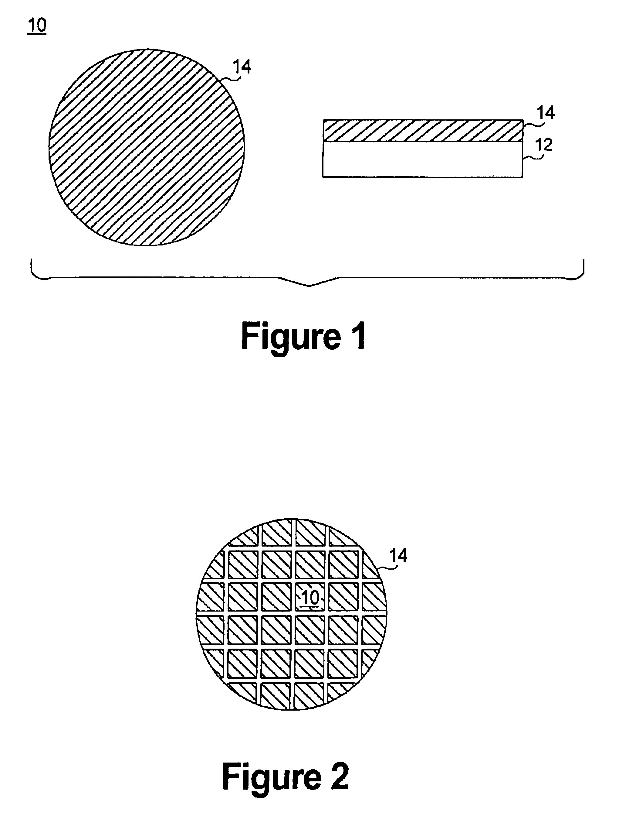
[0033]The present invention provides a methodology for testing an integrated circuit having a test structure integrated with a product structure itself. The test structure and the product structure are integrated in such a manner that a test site occupies some of the product area and the product itself occupies the remainder of the product area.

[0034]This integrated structure maintains an advantage of a localized test structure and has a further advantage of directly duplicating a tool loading for the etch and deposition steps during a manufacture of the integrated circuit. As wafer diameters increase, it becomes more important to duplicate this tool loading factor as closely as possible to ensure that the depositions and etches during the manufacturing process of the integrated circuit behave the same way on the product as they do on the test structure. It is very important that the processing steps be designed for the product and not for the test site since the integrated circuit ...


PUM

PropertyMeasurementUnit
voltageaaaaaaaaaa
stress voltageaaaaaaaaaa
areaaaaaaaaaaa

Abstract

A method and system for predicting gate reliability. The method comprises the steps of stressing a gate dielectric test site to obtain gate dielectric test site data and using the test site data to predict gate reliability. Preferably, the test structure and the product structure are integrated in such a manner that a test site occupies some of the product area and the product itself occupies the remainder of the product area. A preferred methodology, more specifically, is as follows: (1) Test structures at start both in parallel stress mode and in ring oscillator or “product” mode; (2) Analyze the breakdown data as per the present state of the art for each of the areas based on the parallel stress mode; (3) Combine the above breakdown distributions using the area scaling to improve the confidence bounds of the Weibull slope of the cumulative distribution function; (4) Test the ring oscillators in the product mode to determine how many of the stress fails are also product fails as defined by an operational degradation; (5) Subdivide the failures to determine the relationship between the first fail, and the second fail, and the nth fail; (6) Investigate which stress fail, if not the first stress fail, is more likely to cause a product fail as defined by operational degradation; and (7) Based on the subdivision in step 5 and the results in step 6, make projection based on that fail which is most likely to cause fail. The methodology as outlined above bridges between dielectric stress fails and product degradation both in the case of each stress fail causing a product degradation, as well as in the case where more than one stress fail occurs before any product degradation occurs. And this relationship can be quantified.

Description

BACKGROUND OF INVENTION[0001]1. Technical Field[0002]This invention generally relates to the field of reliability testing of integrated circuits. More specifically, the invention relates to a methodology to establish a correlation between gate dielectric test site reliability and product gate reliability.[0003]2. Related Art[0004]In the reliability engineering of integrated circuits, it is necessary to predict product lifetimes and to calculate defect densities. To accomplish this in a short time, product samples may be subjected to environmental conditions that accelerate the failure modes that cause wearout. Typical methods for creating these stress conditions include the use of temperatures and voltages that exceed the operating temperatures and voltages when the circuit is in actual use.[0005]As semiconductor dimensions continue to shrink, the gate dielectric thickness continues to decrease and the voltage is scaled down. The voltage scaling is at a lower rate than is the gate t...

Claims


Application Information

Patent Timeline
Patent Type & Authority Patents(United States)
IPC IPC(8): G01N27/00G01R27/00G01R31/02G01R31/28
CPCG01R31/2855
Inventor BERNSTEIN, KERRYBOLAM, RONALD J.NOWAK, EDWARD J.STRONG, ALVIN W.VAN HORN, JODY J.WU, ERNEST Y.
Owner IBM CORP
Why Eureka
Try Eureka