Fabrication process and layout for magnetic sensor arrays

a technology of magnetic sensor array and fabrication process, which is applied in the field of magnetic sensor array, can solve the problems of large and expensive auxiliary cmos associated with hall effect sensors, inconvenient device design and layout, and inability to meet the needs of the user, so as to achieve more freedom in device design and layout, and reduce the read signal

Active Publication Date: 2012-08-02
EVERSPIN TECHNOLOGIES
View PDF5 Cites 36 Cited by
  • Summary
  • Abstract
  • Description
  • Claims
  • Application Information

AI Technical Summary

Benefits of technology

[0007]A magnetic sensor is configured for enabling independent optimization of the material resistance area (RA) of the MTJ and setting total device resistance so that the total resistance is not so high that Johnson noise becomes a signal limiting concern, and yet not so low that CMOS elements may diminish the read signal. Alternatively, another configuration results in independent optimization of both functions, and more freedom in device design and layout. The X and Y pitch of the sense elements may be arranged such that the line segment that stabilizes, for example, the right side of one sense element; also stabilizes the left side of the adjacent sense element.

Problems solved by technology

While a variety of different sensor types exist for measuring these and other parameters, they all suffer from various limitations.
In order to arrive at the required sensitivity and reasonable resistances that mesh well with CMOS, the sensing units of AMR sensors are generally on the order of square millimeters in size, while the auxiliary CMOS associated with hall effect sensors can similarly become large and expensive.
For mobile applications, such AMR sensor configurations are too costly, in terms of expense, circuit area, and power consumption.
Other types of sensors, such as magnetic tunnel junction (MTJ) sensors and giant magnetoresistance (GMR) sensors, have been used to provide smaller profile sensors, but such sensors have their own concerns, such as inadequate sensitivity and being effected by temperature changes.
However, the magnetic shields are thick and their fabrication requires carefully tuned NiFe seed and plating steps.
Another drawback associated with magnetic shields arises when the shield retains a remnant field when exposed to a strong (˜5 kOe) magnetic field, since this remnant field can impair the low field measuring capabilities of the bridge structure.
To prevent the use of magnetic shields, a Wheatstone bridge structure may include two opposite anti-ferromagnetic pinning directions for each sense axis, resulting in four different pinning directions which must be individually set for each wafer, very often requiring complex and unwieldy magnetization techniques.
The resistance of the reset line limits the line run length while allowing pulses of sufficient reset current from a fixed voltage overhead and therefore limits the array size.

Method used


Image

  • Fabrication process and layout for magnetic sensor arrays
  • Fabrication process and layout for magnetic sensor arrays
  • Fabrication process and layout for magnetic sensor arrays

Examples


Embodiment Construction

[0028]The following detailed description is merely illustrative in nature and is not intended to limit the embodiments of the subject matter or the application and uses of such embodiments. Any implementation described herein as exemplary is not necessarily to be construed as preferred or advantageous over other implementations. Furthermore, there is no intention to be bound by any expressed or implied theory presented in the preceding technical field, background, brief summary, or the following detailed description.

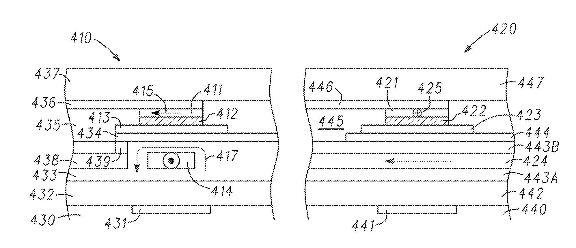
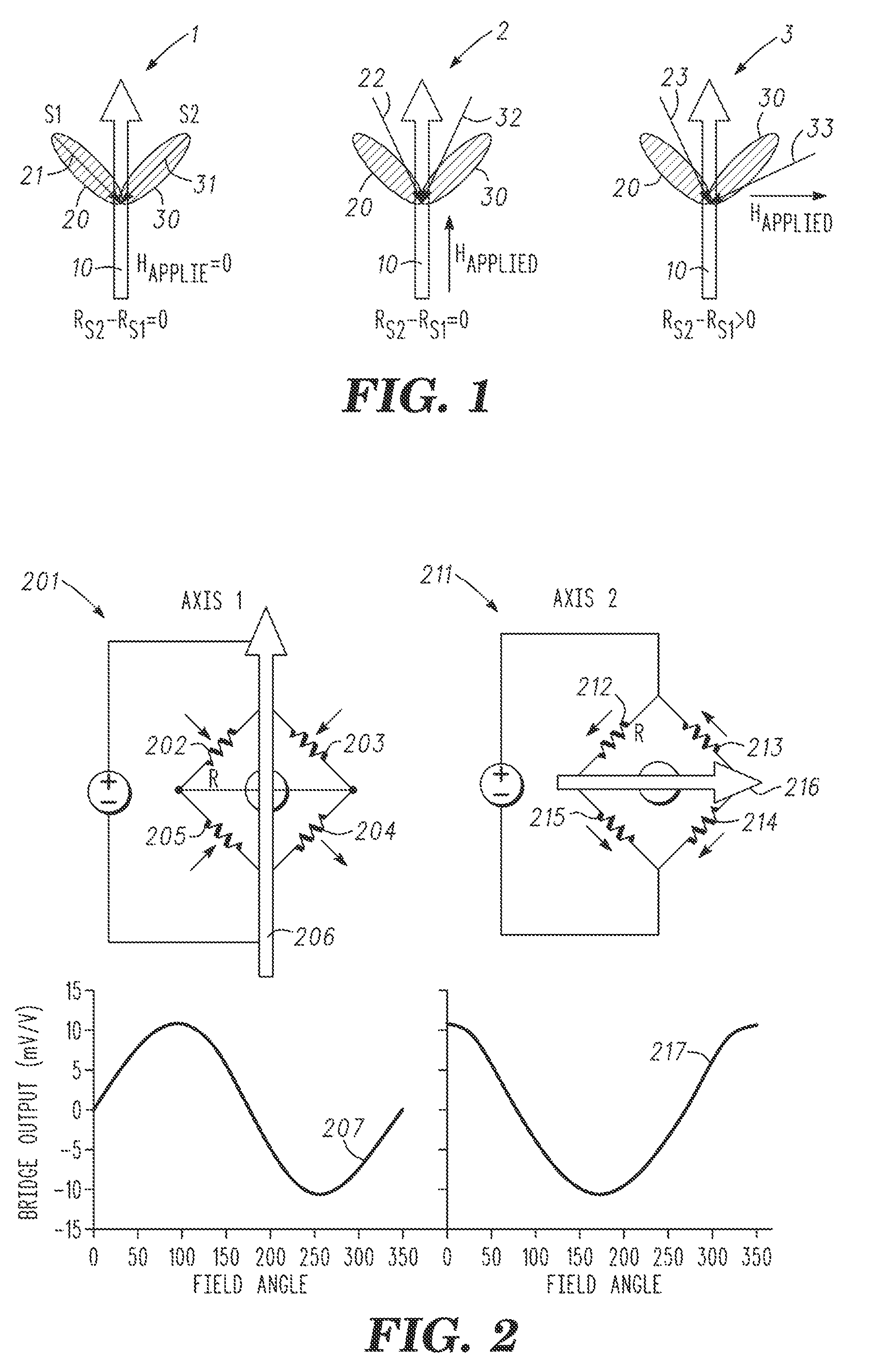
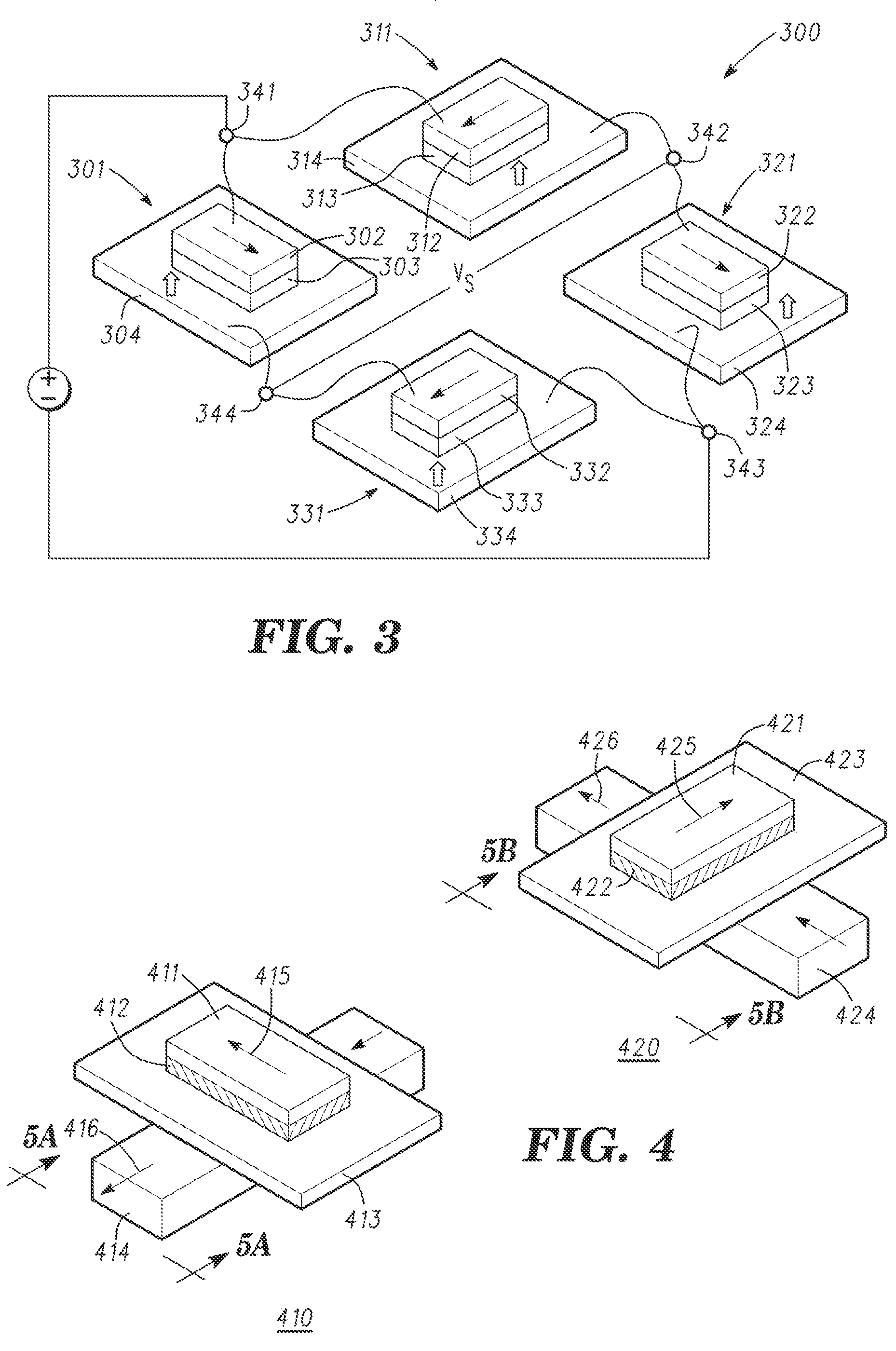
[0029]A magnetic field sensing device includes, for example at least one Wheatstone bridge, wherein each leg comprises an array of magnetic tunnel junctions (MTJs). Each MTJ includes a reference layer, a tunnel barrier (TB), and a sense layer (or sense element). For the highest signal to noise ratio in a given chip area (the densest packing of sense elements), groups of these MTJs may share a common reference layer. The shape of the reference layer may optionally be conf...


PUM


Abstract

A magnetic sensor includes a plurality of groups, each group comprising a plurality of magnetic tunnel junction (MTJ) devices having a plurality of conductors configured to couple the MTJ devices within one group in parallel and the groups in series enabling independent optimization of the material resistance area (RA) of the MTJ and setting total device resistance so that the total bridge resistance is not so high that Johnson noise becomes a signal limiting concern, and yet not so low that CMOS elements may diminish the read signal. Alternatively, the magnetic tunnel junction devices within each of at least two groups in series and the at least two groups in parallel resulting in the individual configuration of the electrical connection path and the magnetic reference direction of the reference layer, leading to independent optimization of both functions, and more freedom in device design and layout. The X and Y pitch of the sense elements are arranged such that the line segment that stabilizes, for example, the right side of one sense element; also stabilizes the left side of the adjacent sense element.

Description

[0001]This application claims the benefit of U.S. Provisional Application No. 61 / 438,007 filed 31 Jan. 2011.TECHNICAL FIELD[0002]The exemplary embodiments described herein generally relates to the field of magnetoelectronic devices, and more particularly to CMOS compatible magnetoelectronic field sensors used to sense magnetic fields.BACKGROUND[0003]Sensors are widely used in modern systems to measure or detect physical parameters, such as position, motion, force, acceleration, temperature, pressure, etc. While a variety of different sensor types exist for measuring these and other parameters, they all suffer from various limitations. For example, inexpensive low field sensors, such as those used in an electronic compass and other similar magnetic sensing applications, generally are Hall effect devices with flux concentrators or anisotropic magnetoresistance (AMR) based devices. In order to arrive at the required sensitivity and reasonable resistances that mesh well with CMOS, the s...

Claims


Application Information

Patent Timeline
Patent Type & Authority Applications(United States)
IPC IPC(8): H01L29/82H01L21/02
CPCG01R33/098H01L43/12H01L43/08H01L27/22H10B61/00H10N59/00H10N50/10H10N50/80H10N50/01
Inventor MATHER, PHILLIPSLAUGHTER, JONRIZZO, NICHOLAS
Owner EVERSPIN TECHNOLOGIES
Why Eureka
Try Eureka