
Process for producing solid electrolytic capacitor and solid electrolytic capacitor

a solid electrolytic capacitor and electrolytic capacitor technology, which is applied in capacitor manufacture, capacitor casing/cabinet/drawer details, electrical apparatus casings/cabinets/drawers, etc., can solve the problems of inefficient plating step twice in fabricating solid electrolytic capacitors, structural limitations of capacitors such as these, and achieve high strength.

Active Publication Date: 2005-05-10
SANYO ELECTRIC CO LTD +1
View PDF5 Cites 35 Cited by
  • Summary
  • Abstract
  • Description
  • Claims
  • Application Information

AI Technical Summary

Benefits of technology

[0013]When the anode terminal member and the cathode terminal member are cut, the inner end portions of the members separated from the frame provide an anode terminal and a cathode terminal for the capacitor. The plating step forms a plating layer in regions at least inwardly of the vertical planes, and the anode terminal member and the cathode terminal member are cut along the vertical planes through the respective holes or cavities, so that the inner surfaces of the terminal members defining the holes or cavities and providing side portion of the anode terminal and the cathode terminal are covered with the plating layer. This obviates the need to plate the terminals after the capacitor is cut off from the fabrication frame. Thus, the solid electrolytic capacitor of the chip type having no electrodes extending outward and bent can be fabricated by a process which is similar to the conventional process for producing solid electrolytic capacitors. Since the packaging resin portion is formed without permitting the resin to ingress into the holes or cavities and therefore leaving the holes or cavities, there is no need to protect the terminal regions as with an insulating layer, with the result that the capacitor can be obtained when the anode terminal member and the cathode terminal member are cut.
[0014]The present invention provides a solid electrolytic capacitor which is fabricated by the above process and in which a recess is formed in a side portion of each of the anode terminal and the cathode terminal. Since the recesses are open at least downward, the solder used for mounting the capacitor on a board forms heaps as joined to the bottom surfaces of the recesses. A plating layer is formed on the bottom surfaces of the recesses and therefore serves to mount the capacitor on the board with a high strength. The flow of the solder as melted for soldering is restrained by the recesses, which accordingly prevent the molten solder from flowing onto the packaging resin portion. Consequently, the solid electrolytic capacitor can be mounted on the board promptly with safety without the necessity of paying attention to an outflow of the solder.

Problems solved by technology

However, with a growing demand for compacted chip-type solid electrolytic capacitors of lower ESR, capacitors of such type encounter structural limitations.
The capacitor fabricating process described above is cumbersome because the process includes the step of masking the cathode terminal 35 with the insulator 36a and the step of removing the insulator 36a after the packaging resin portion 34 has been formed.
Nevertheless, the following problem is encountered in the case where solid electrolytic capacitors of the type mentioned are fabricated by a process similar to the conventional process.
However, performing the plating step twice in fabricating the solid electrolytic capacitor is inefficient, while plating the capacitors individually after the separating step is extremely cumbersome.

Method used


Image

  • Process for producing solid electrolytic capacitor and solid electrolytic capacitor
  • Process for producing solid electrolytic capacitor and solid electrolytic capacitor
  • Process for producing solid electrolytic capacitor and solid electrolytic capacitor

Examples


Embodiment Construction

[0025]With reference to the drawings concerned, a description will be given of a first embodiment of the invention, i.e., a process for fabricating a chip-type solid electrolytic capacitor. Throughout the drawings, like parts will be designated by like reference numerals.

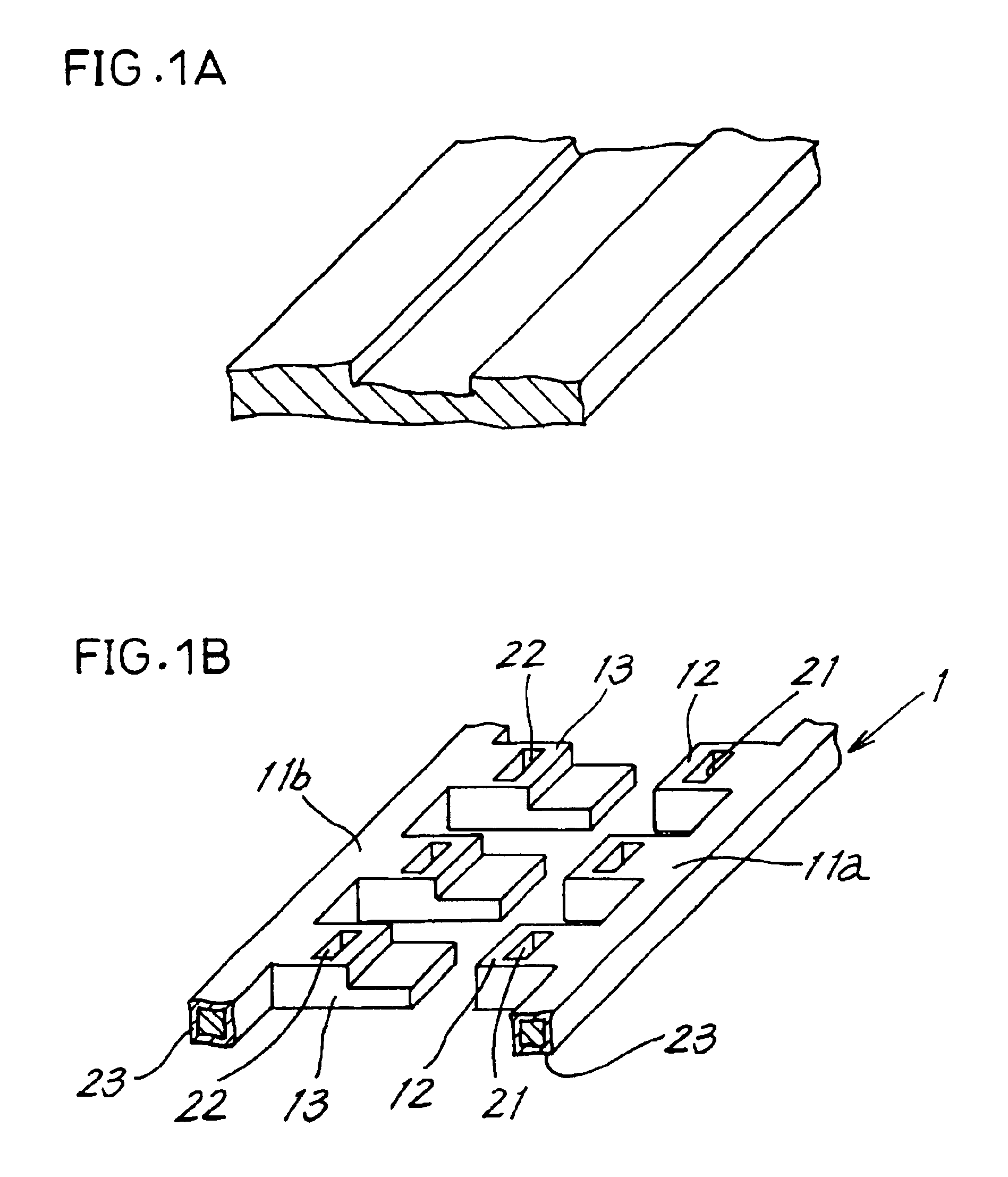
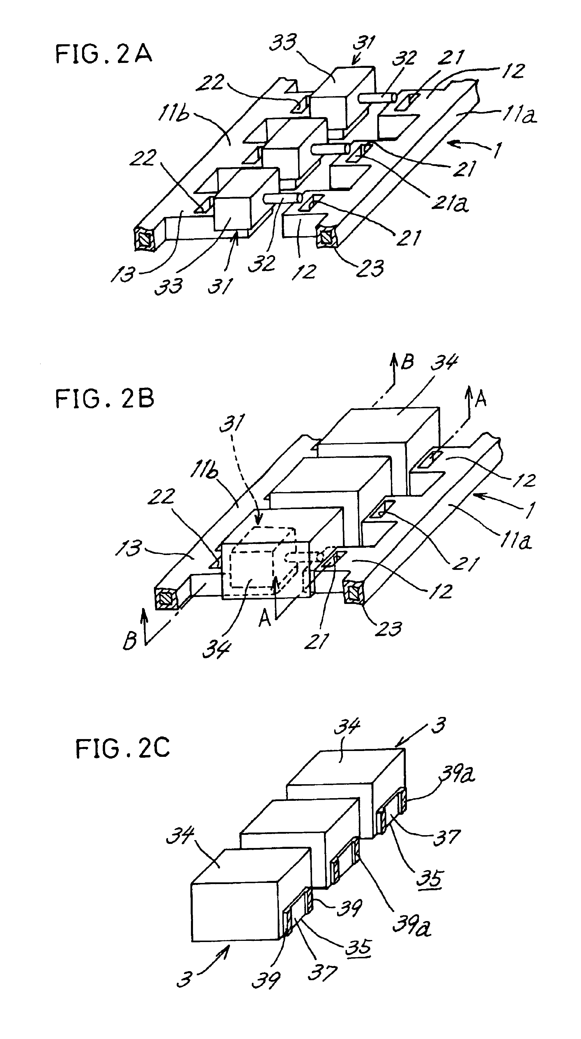
[0026]Steps of making a fabrication frame 1 will be described with reference to FIGS. 1A and 1B.

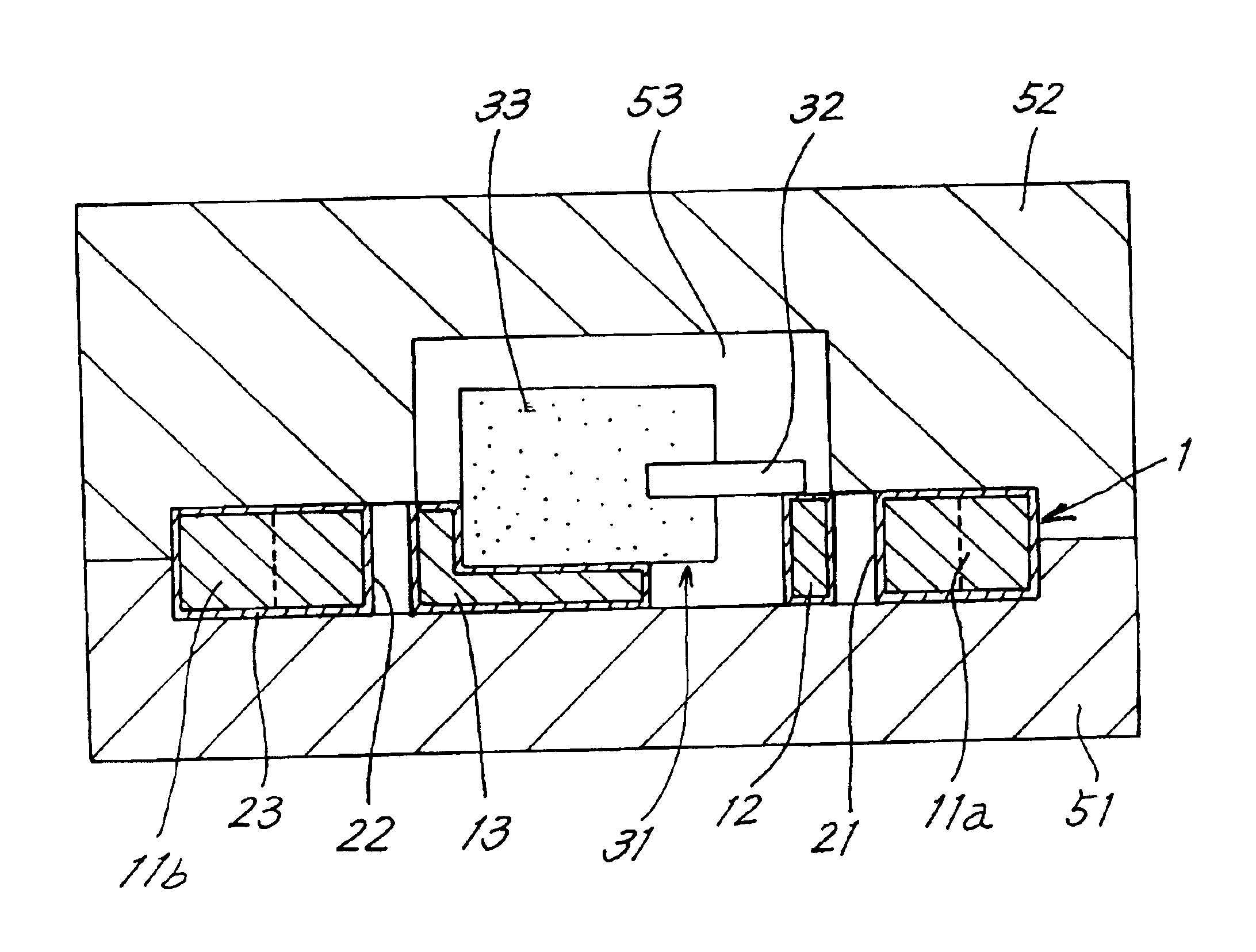
[0027]First as shown in FIG. 1A, a striplike recessed portion is formed approximately in the center of upper surface of a metal thin plate (e.g., a copper plate having a thickness of about 0.3 mm) longitudinally thereof. The drawing shows only a portion of the thin plate. Next, a fabrication frame 1 shown in FIG. 1B is made from the thin plate by press work (blanking). The fabrication frame 1 has a pair of side frame members 11a, 11b extending longitudinally thereof. Anode terminal members 12 project inward from the side frame member 11a, and cathode terminal members 13 project inward from the other side frame member 11b ...


PUM


Abstract

The invention provides a process for fabricating a solid electrolytic capacitor of the chip type which process includes the steps of plating a fabrication frame comprising an anode terminal member and a cathode terminal member projecting from a pair of side frame members respectively so as to be opposed to each other, the anode terminal member being stepped so as to provide a lower portion toward the cathode terminal member, a hole extending vertically and being formed in each of the anode terminal member and a higher portion of the cathode terminal member, joining an anode lead of a capacitor element to an upper surface of the cathode terminal member and a bottom surface of the capacitor element to an upper surface of the lower portion of the cathode terminal member, forming a packaging resin portion around the capacitor element without permitting resin to ingress into the holes, and cutting the anode and cathode terminal members along vertical planes extending through the respective holes.

Description

FIELD OF THE INVENTION[0001]The present invention relates to a process for fabricating a solid electrolytic capacitor comprising a capacitor element packaged with a resin layer, and the solid electrolytic capacitor produced by this process.BACKGROUND ART[0002]Solid electrolytic capacitors of the chip type comprise a capacitor element including a sintered block which has one end of an anode lead embedded therein and which is provided with an insulating layer, electrolyte layer and cathode layer formed over the surface of the block. Common chip-type solid electrolytic capacitors are fabricated by joining a terminal in the form of a thin plate to each of the anode lead and the cathode layer, forming a packaging resin portion around the capacitor element by resin molding and thereafter bending the terminals so as to position the outer ends of the terminals beneath the bottom of the resin portion. However, with a growing demand for compacted chip-type solid electrolytic capacitors of low...

Claims


Application Information

Patent Timeline
IPC IPC(8): H01G9/00H01G9/004H01G13/00H01G9/15H01G2/12H01G9/012
CPCH01G9/012H01G9/15H01G11/56Y10T29/417Y02E60/13
Inventor FUJII, EIZOISHIDA, HIDEKI
Owner SANYO ELECTRIC CO LTD
Features
  • Generate Ideas
  • Intellectual Property
  • Life Sciences
  • Materials
  • Tech Scout
  • Unparalleled Data Quality
  • Higher Quality Content
  • 60% Fewer Hallucinations
Learn More