Circuit housing

a circuit housing and circuit technology, applied in the direction of casings/cabinets/drawers, hermetically sealed casings, casings/cabinets/drawers details of electrical appliances, etc., can solve the problems of rigid and permanent connection between materials, and achieve the effect of eliminating a technologically elaborate processing step, ensuring the reliability of contact with the chip, and ensuring the integrity of the connection

Inactive Publication Date: 2005-05-10
F&K DELVOTEC BONDTECHN
View PDF13 Cites 18 Cited by
  • Summary
  • Abstract
  • Description
  • Claims
  • Application Information

AI Technical Summary

Benefits of technology

[0016]The term “contact surfaces” in the context of the invention is understood to mean both genuine surface contact sites (pads) and also—in an embodiment that may even be preferred—low, flat elevations made of a well-conducting and corrosion-resistant material, in particular gold. Slight elevations of this kind can in particular be formed by stamping (“flattening”) small gold spheres similar to the customary bumps. This embodiment ensures a higher reliability of contacting the chip within the housing, with respect to higher tolerances of the bump configuration or of slight curvatures or distortions of the housing or chip surfaces.
[0017]A substantial advantage of the solution proposed here is that the chip does not need to be soldered to the housing, or eutectically connected to its contact surfaces or elements, which eliminates a technologically elaborate processing step. Because the materials of chip and housing are not fixedly (and hence rigidly) joined together, the present quality problems resulting from different thermal expansion coefficients no longer arise, for practical purposes. Furthermore, the housing can be tested immediately (and closed or finished only after the test has been passed), and repairs can be carried out in a cost-effective manner, without discarding the expensive chip.
[0023]The above-mentioned gas-tight seal advantageously enables the interior of the housing to be permanently filled with a medium that is slow to react, in particular an inert gas, which reliably prevents any corrosive processes from operating inside the housing.
[0025]To prevent forces of external origin being transmitted to the chip, the lid of the housing is preferably rigidly constructed and, where appropriate, is connected to the wall in such a way that external forces are reliably absorbed. The same function can be served by a protective roofing structure that provides a rigid covering (for example, is made of a hardened, loaded artificial resin).

Problems solved by technology

That is, these problems are basically brought about by the difficulty of producing a rigid, permanent connection between materials having very different thermal expansion coefficients.

Method used


Image

  • Circuit housing
  • Circuit housing
  • Circuit housing

Examples


Embodiment Construction

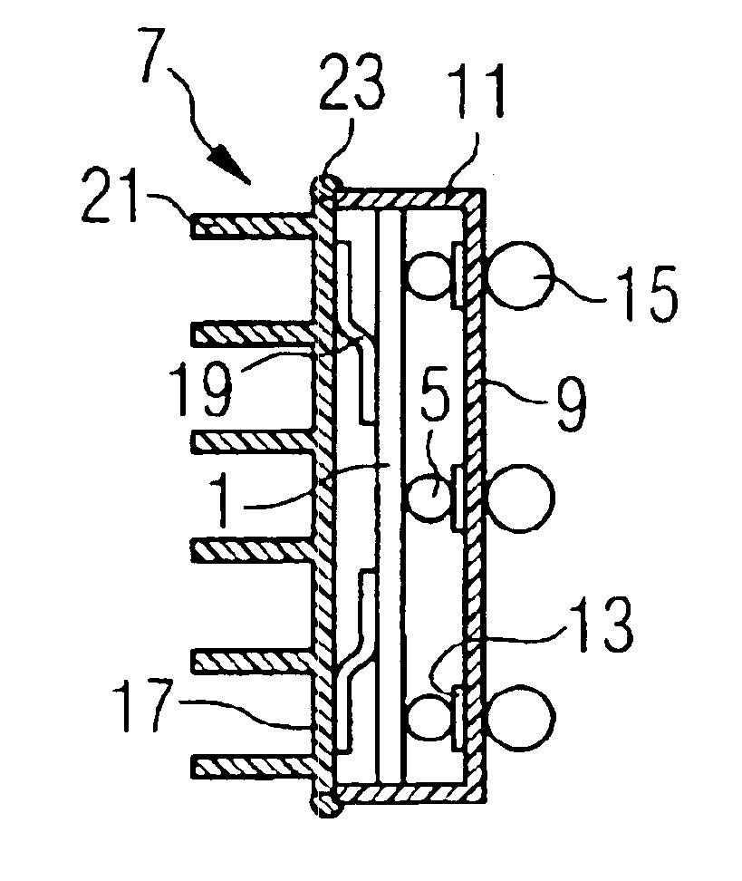
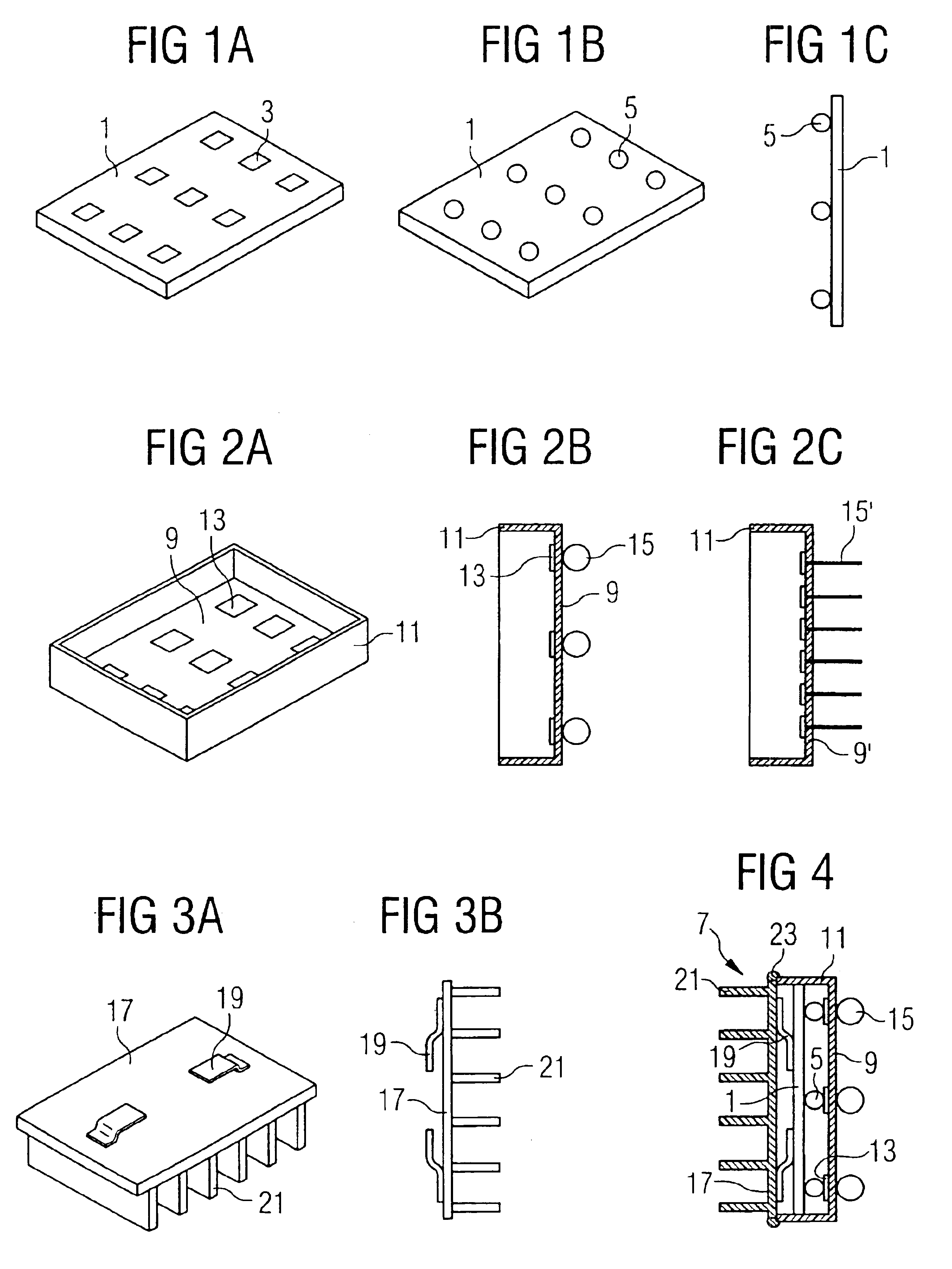
[0038]FIGS. 1A to 4 show—in rough schematic drawings—a semiconductor chip 1 with metallic contact surfaces 3 and gold contact elements (bumps) 5, which is to be encapsulated in a miniaturized chip housing 7. The shape of the latter corresponds to the basic rectangular form of the chip, in that it has a rectangular housing floor 9 with integral low wall 11, on the inner surface of which metallic contact surfaces 13 are likewise provided and which has on its under (outer) surface soldered contact elements (solder balls) 15 or—in the modified embodiment according to FIG. 2C—contact pins 15′ as housing contact elements. (Because in the embodiment according to FIG. 2C the housing floor is of course correspondingly modified, there it is identified by the reference numeral 9′.) The housing 7 further comprises a lid 17, a flat rectangular structure of the same shape as the floor 9, which in its middle region bears two metallic spring elements (leaf springs) 19 on its lower surface and cooli...


PUM


Abstract

Miniaturized circuit housing to encapsulate and provide external contacts for at least one integrated circuit, in particular of the flip-chip or wafer-level-package type, with a housing floor, the lower surface of which bears housing contact elements for making external contact and the upper surface of which is electrically connected to circuit contact elements on the lower surface of the circuit, wherein a housing lid is provided, in particular opposite the housing floor, which presses the circuit with the circuit contact element resiliently against the upper surface of the housing floor, and between the circuit contact elements and the housing floor there is no connection that fixes their materials permanently together.

Description

[0001]Related Applications This application claims the benefit of the application 01 115 832.6 filed in the European Patent Office Jun. 28, 2001.BACKGROUND OF THE INVENTION[0002]1. Field of the Invention[0003]The invention relates to a miniaturized circuit housing for encapsulating and providing external contacts for integrated circuits and, in particular, a housing with a housing floor and an oppositely disposed housing lid which presses a circuit contact element positioned therebetween resiliently against the upper surface of the housing floor.[0004]2. Description of the Related Art[0005]Integrated circuits (chips) employed in electronic devices are almost always mounted in housings. These housings protect the sensitive semiconductor structures from harmful environmental influences such as moisture, light, dust and mechanical forces. In many cases enclosure in a housing simultaneously serves to adapt the structural widths and distances customary in LSI and VLSI technology to the—s...

Claims


Application Information

Patent Timeline
Patent Type & Authority Patents(United States)
IPC IPC(8): H01L23/48H05K5/00H01L23/02H01L23/043H05K5/03H05K5/06H05K7/20
CPCH01L24/72H01L2924/01072H01L2924/01002H01L2924/01004H01L2924/01018H01L2924/01078H01L2924/01079H01L2924/01082H01L2924/01322H01L2924/14H01L2924/15312H01L2924/19043H01L2924/3025H01L2924/01005H01L2924/01006H01L2924/01033H01L2924/01068H01L2224/16H01L24/13H01L24/16H01L2224/73251H01L2224/72H01L23/043
Inventor FARASSAT, FARHAD
Owner F&K DELVOTEC BONDTECHN
Why Eureka
Try Eureka