Dual source lithography for direct write application

a lithography and write application technology, applied in the field of lithography, can solve the problems of increasing the capital cost of photomasks employing resolution enhancement techniques, increasing the cost of masks to produce resolution enhancement techniques (ret's), and increasing the cost of suitable phase shift masks nearly an order of magnitude more than a standard binary mask, so as to achieve high throughput and increase the net throughput

Inactive Publication Date: 2005-05-17
BELL SEMICON LLC
View PDF1 Cites 28 Cited by
  • Summary
  • Abstract
  • Description
  • Claims
  • Application Information

AI Technical Summary

Problems solved by technology

But the mask cost to produce resolution enhancement techniques (RET's) is growing exponentially.
For example, suitable phase shift masks costs nearly an order of magnitude more than a standard binary mask (i.e., a mask without resolution enhancement).
Increased capital costs for photomasks employing resolution enhancement techniques will likely have disparate impacts on the semiconductor industries.
But direct write lithography is very slow.
Conventional lithography can process up to 100 wafers / hour, but direct write lithography may take as long as a day to process one wafer.
Extended write times also create CD control and defect issues and are not practical at the current time.

Method used


Image

  • Dual source lithography for direct write application
  • Dual source lithography for direct write application
  • Dual source lithography for direct write application

Examples


Embodiment Construction

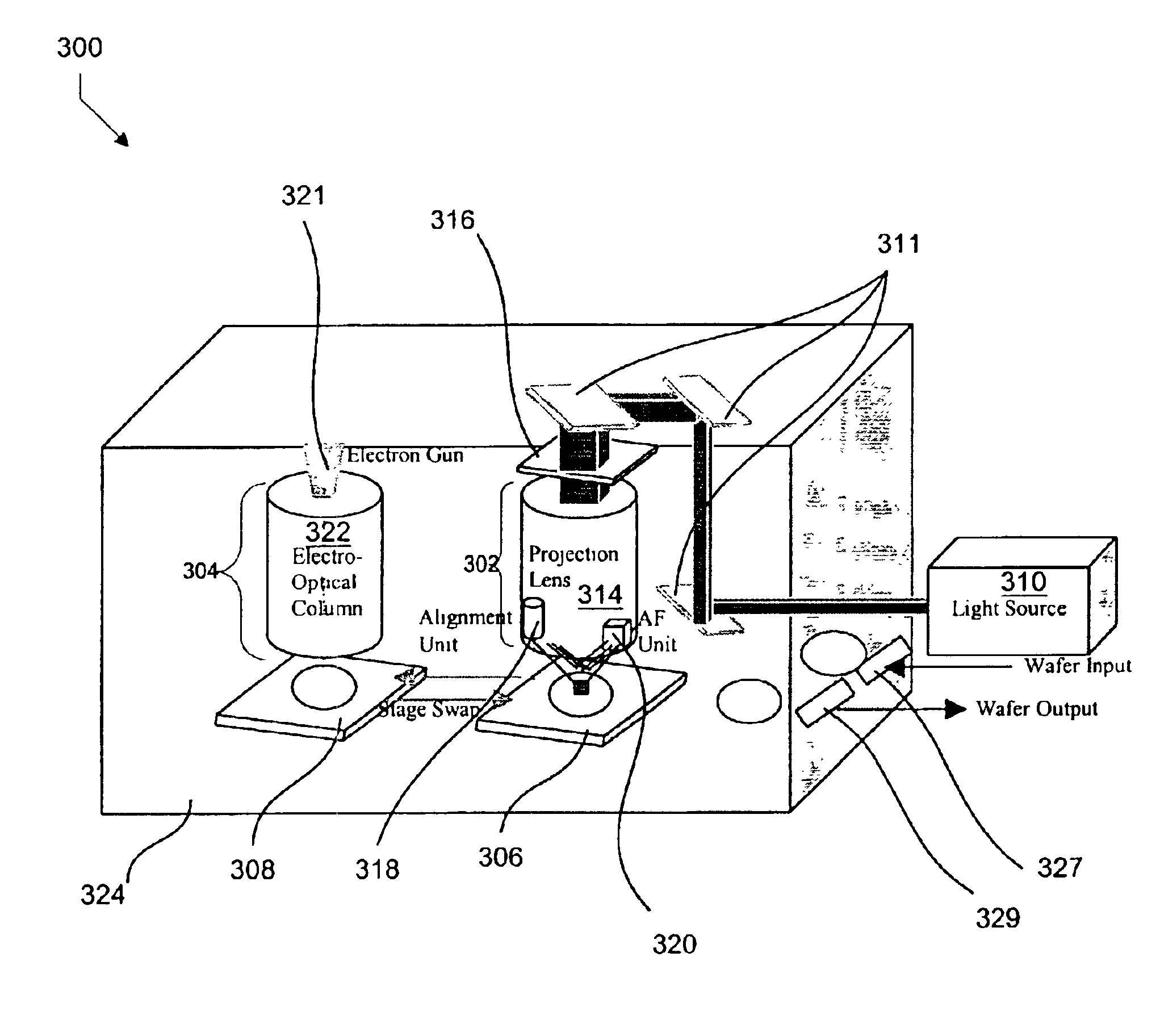
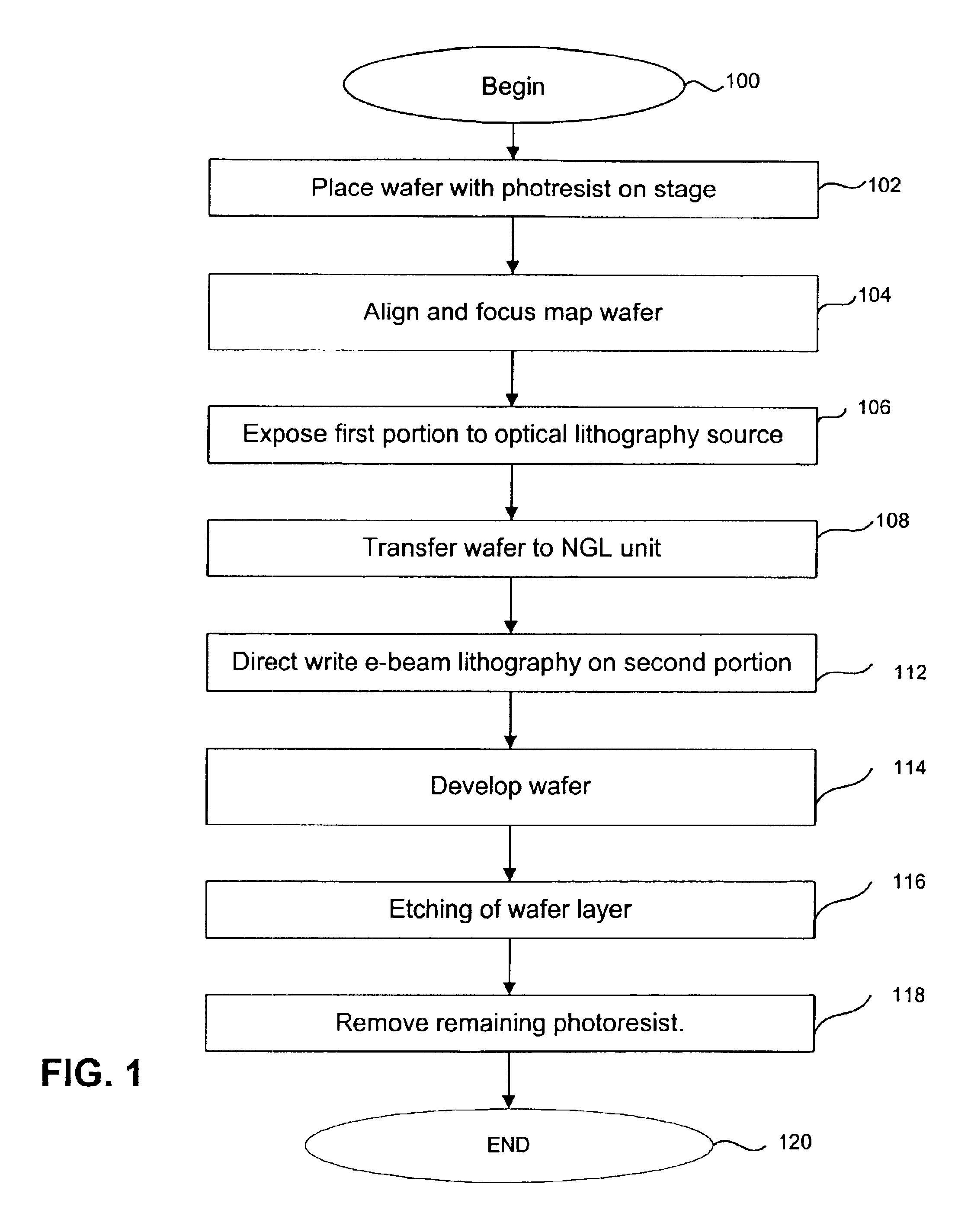
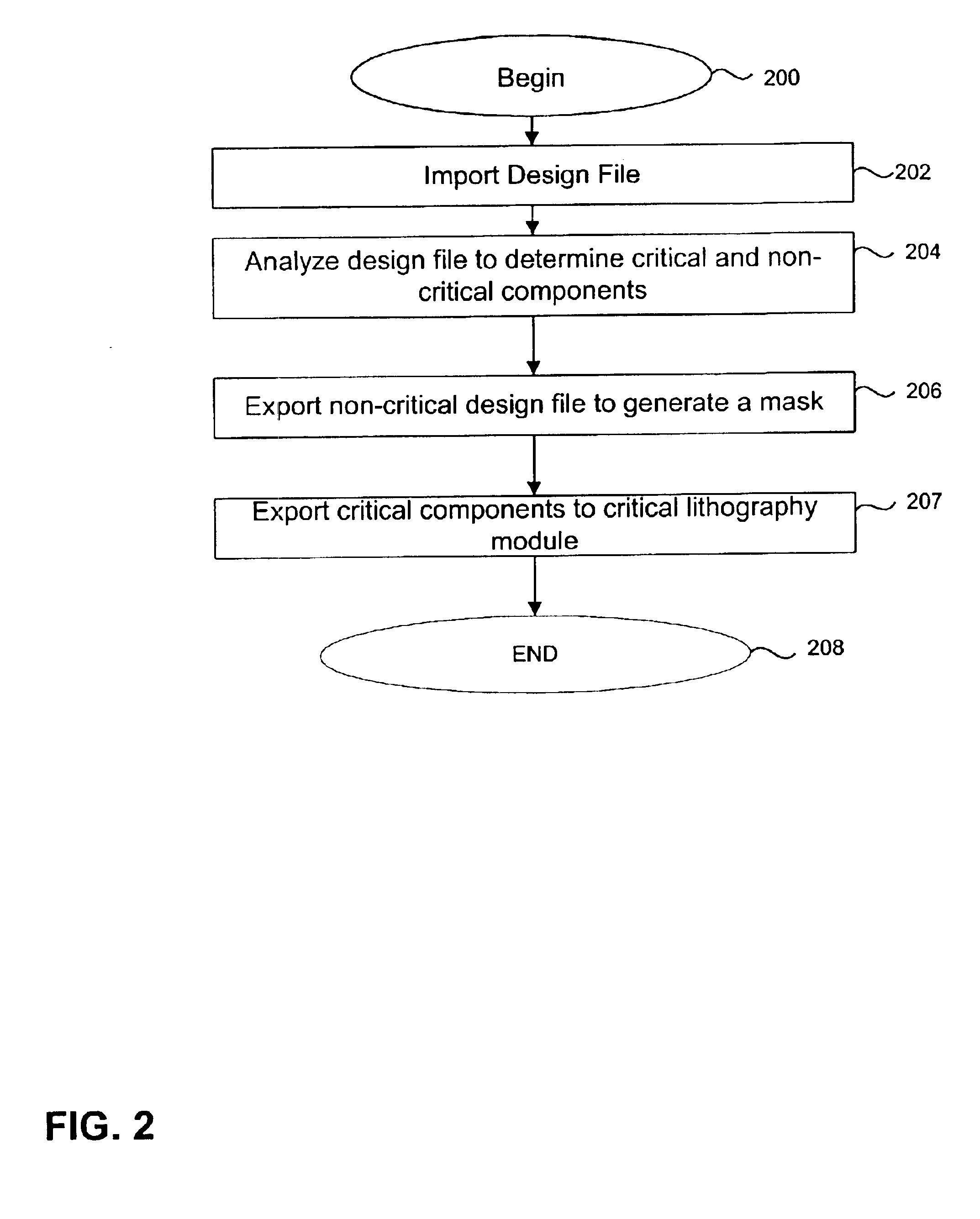
[0018]Reference will now be made in detail to preferred embodiments of the invention. Examples of the preferred embodiments are illustrated in the accompanying drawings. While the invention will be described in conjunction with these preferred embodiments, it will be understood that it is not intended to limit the invention to such preferred embodiments. On the contrary, it is intended to cover alternatives, modifications, and equivalents as may be included within the spirit and scope of the invention as defined by the appended claims. In the following description, numerous specific details are set forth in order to provide a thorough understanding of the present invention. The present invention may be practiced without some or all of these specific details. In other instances, well known process operations have not been described in detail in order not to unnecessarily obscure the present invention.

[0019]The present invention in various embodiments provides a dual source lithograph...


PUM

PropertyMeasurementUnit
thresholdaaaaaaaaaa
vacuumaaaaaaaaaa
sizeaaaaaaaaaa

Abstract

A dual exposure source lithography system forms a first and a second portion of a pattern on a wafer. An optical lithography module forms the first portion of the pattern. A non-optical lithography module forms the second portion of the pattern using a non-optical lithography exposure source. The non-optical exposure source is an electron beam lithography source, an EUV source, an x-ray source, or another next generation lithography system exposure source. A mask design file is decomposed into separate design files reflecting critical and non-critical components of the pattern to be formed on the wafer.

Description

BACKGROUND OF THE INVENTION[0001]1. Field of the Invention[0002]The present invention relates to lithography of semiconductor wafers. More particularly, the present invention relates to lithography using two lithography exposure sources to form a pattern.[0003]2. Description of the Related Art[0004]Semiconductor wafer fabrication involves a series of processes used to create semiconductor devices and integrated circuits (ICs) in and on a semiconductor wafer surface. Fabrication typically involves the basic operations of layering and patterning, together with others such as doping, and heat treatments. Layering is an operation used to add thin layers of material (typically insulator, semi-conductor or conductor) to the surface of the semiconductor wafer. Patterning is an operation that is used to remove specific portions of the top layer or layers on the wafer surface. Patterning is usually accomplished through the use of photolithography (also known as photomasking) to transfer the ...

Claims


Application Information

Patent Timeline
Patent Type & Authority Patents(United States)
IPC IPC(8): G03B27/44G03B27/32G03B27/54G03F7/20H01J37/317
CPCB82Y10/00B82Y40/00G03F7/7045H01J37/3174G03F7/70383H01J2237/31757
Inventor BERMAN, MICHAEL J.BAILEY, GEORGE E.
Owner BELL SEMICON LLC
Why Eureka
Try Eureka