Pattern forming method

Inactive Publication Date: 2005-05-24
FUJITSU LTD
View PDF6 Cites 12 Cited by
  • Summary
  • Abstract
  • Description
  • Claims
  • Application Information

AI Technical Summary

Benefits of technology

[0017]According to the present invention, positions of the LSI chips with respect to the core substrate are detected, the pattern data for a pattern to be formed on the core substrate is corrected based on positional information of the LSI chips, a mask pattern based on the corrected pattern data is dis

Problems solved by technology

However, according to the above-described method for fabricating the conventional package substrate, in which a multi-level interconnection layer is formed on a substrate with LSI chip embedded in, a plurality of LSI chips embedded in a core substrate are often independently disaligned.
Higher accuracy for the alignment is required for a larger number of LSI chips, which makes it difficult to control the alignment ac

Method used


Image

  • Pattern forming method
  • Pattern forming method
  • Pattern forming method

Examples


Embodiment Construction

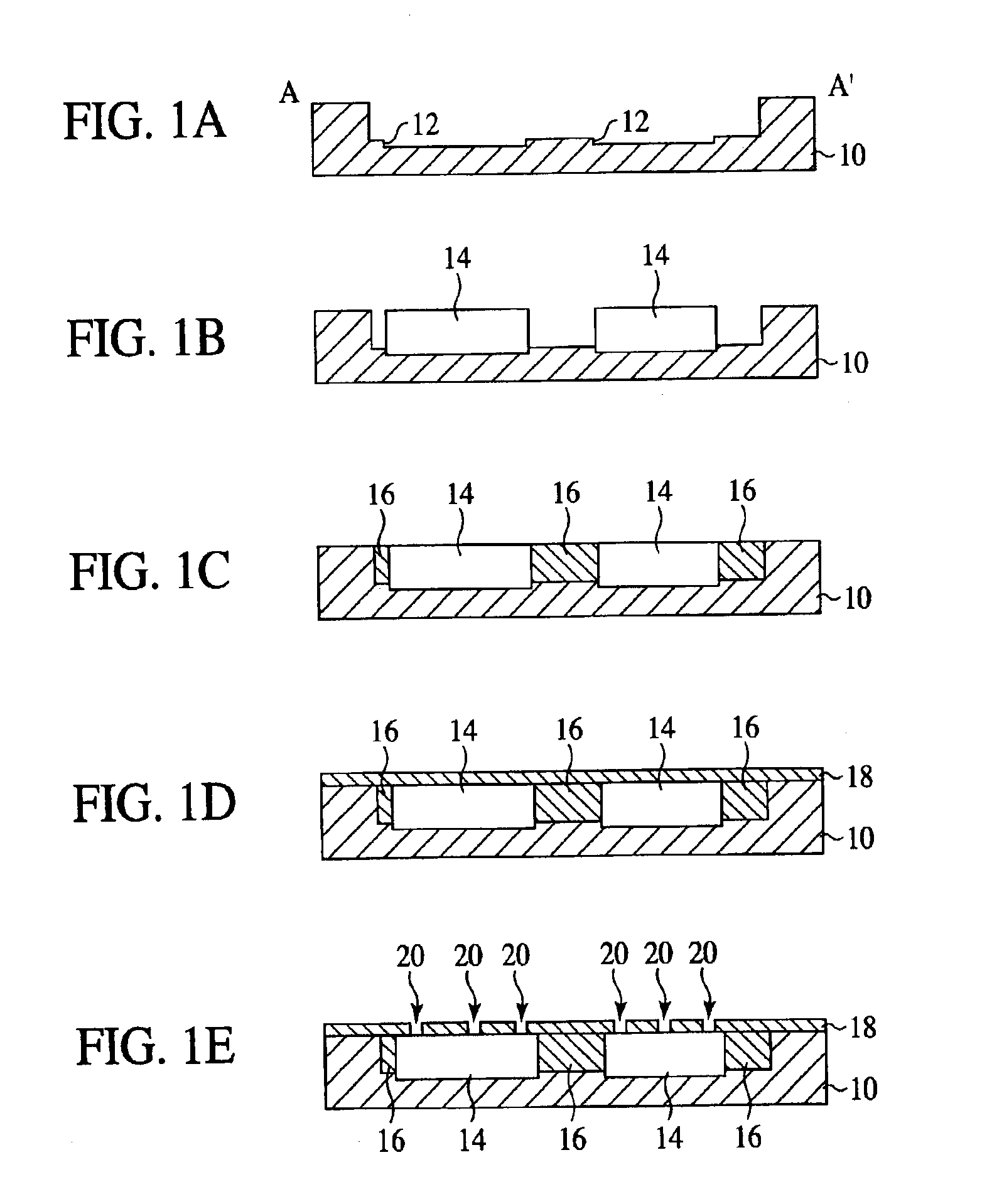
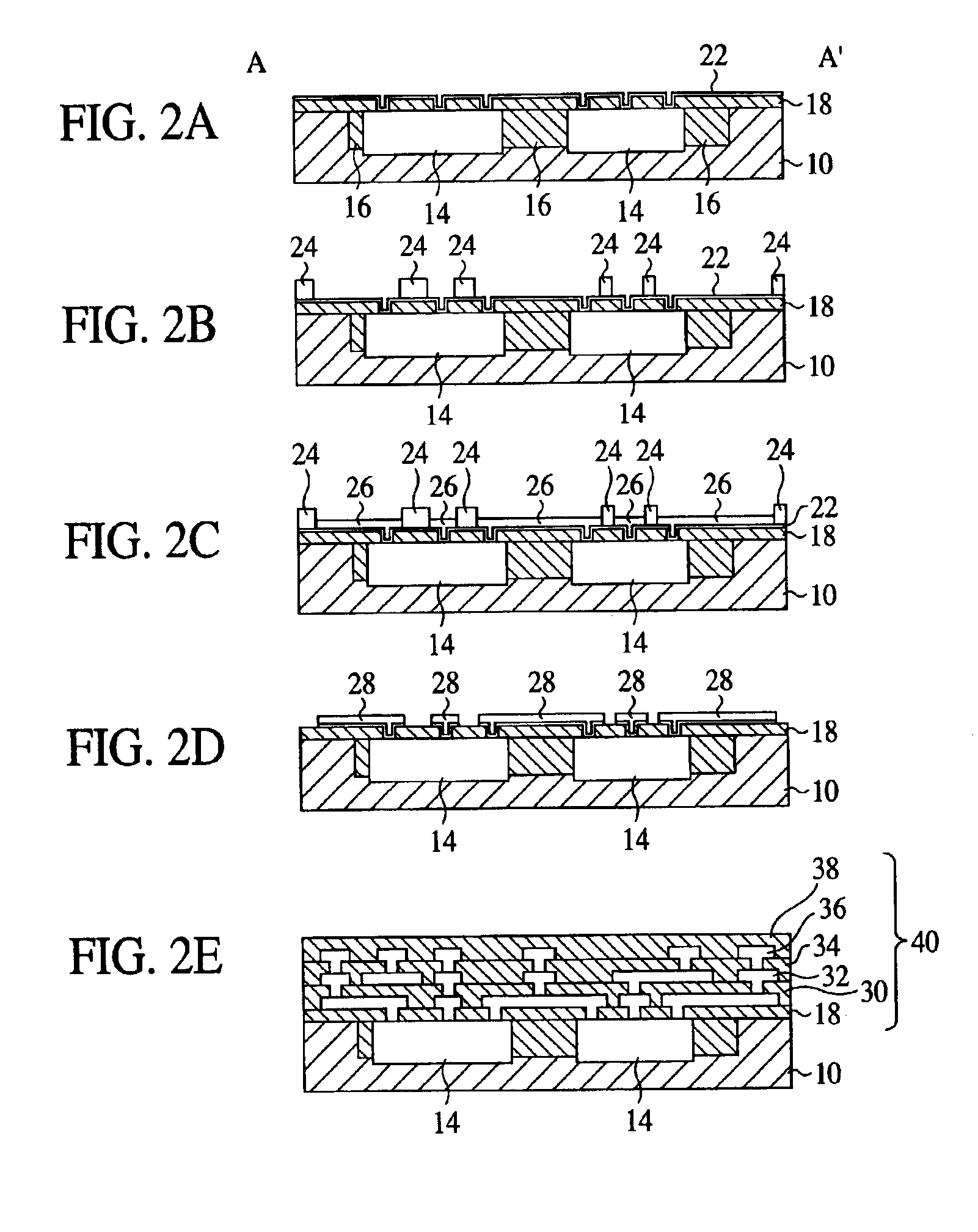
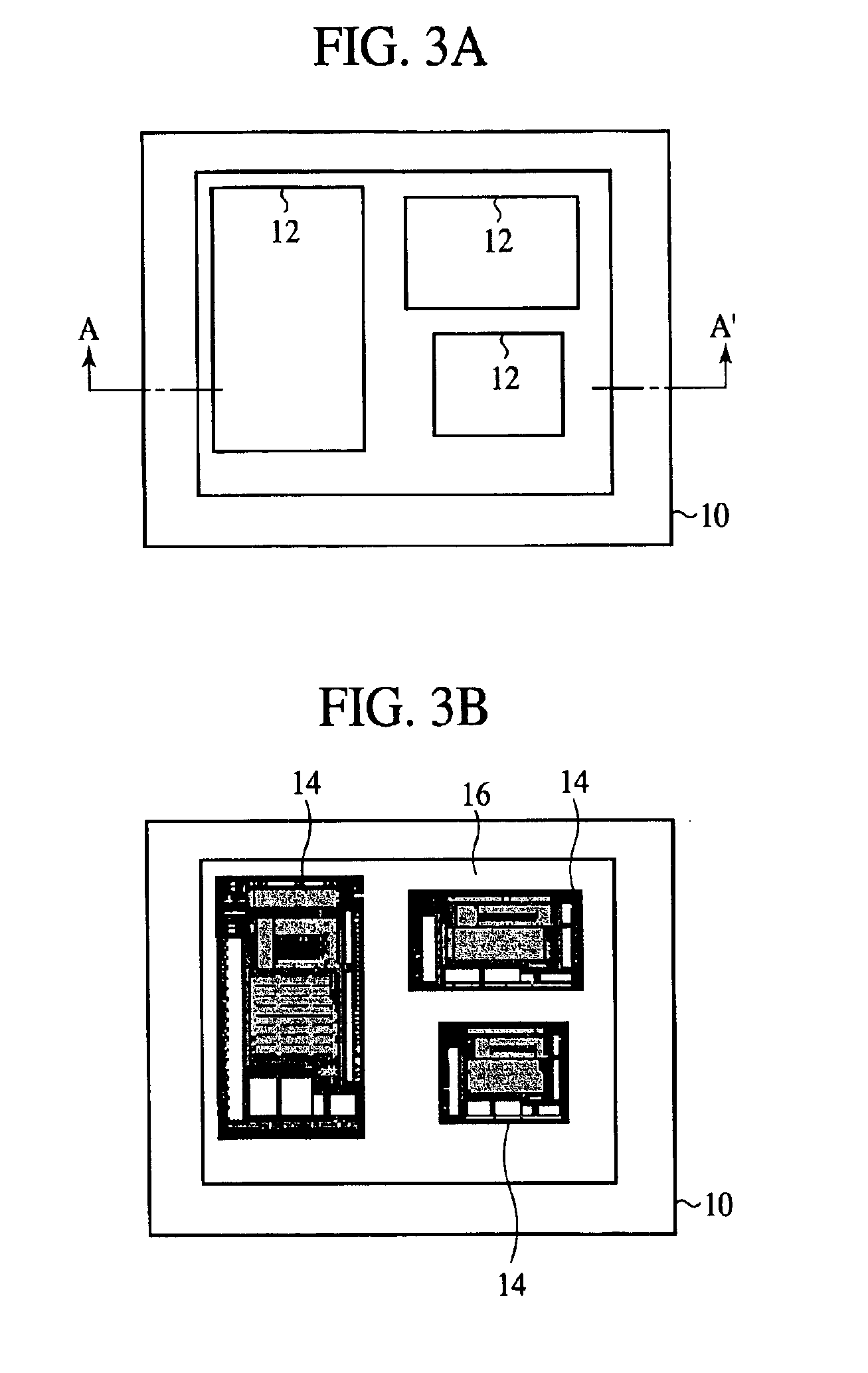
[0023]The pattern forming method according to one embodiment of the present invention will be explained with reference to FIGS. 1A-1E, 2A-2E, 3A-3B, 4 and 5A-5B.

[0024]FIGS. 1A-1E and 2A-2E are sectional views of a package substrate in the steps of the pattern forming method according to the present embodiment, which explain the method. FIGS. 3A and 3B are plan views showing the pattern forming method according to the present embodiment. FIG. 4 is a plan view showing one example of disalignment of LSI chips. FIGS. 5A and 5B are plan views of one example of a basic mask pattern and the mask pattern as corrected.

[0025]Grooves 12 for a plurality of LSI chips to be embedded in are formed in a core substrate 10 to be the base (FIG. 1A, FIG. 3A). In place of forming the grooves 12, a core substrate with mold frames for the LSI chips to be embedded in may be used.

[0026]Then, LSI chips 14 are fit in the grooves 12 formed in the core substrate 12 and secured with a resin (FIG. 1B). The LSI ch...


PUM


Abstract

A pattern forming method comprising the steps of: detecting a position of a base pattern formed on a substrate; forming a photosensitive resin film on the substrate; correcting a pattern data of a pattern to be formed on the substrate, based on a positional information of the base pattern to thereby compute a corrected pattern data; displaying a mask pattern on a liquid crystal panel, based on the corrected pattern data; and exposing the photosensitive resin film with the liquid crystal panel as a mask and developing the same to thereby pattern the photosensitive resin film. Even when a base pattern has rotations, shrinkages, distortions, etc., a prescribed upper layer pattern can be formed in alignment with the lower layer pattern.

Description

CROSS-REFERENCE TO RELATED APPLICATIONS[0001]This application is based upon and claims the benefit of priority from the prior Japanese Patent Application No. 2001-384297, filed in Dec. 18, 2001, the entire contents of which are incorporated herein by reference.BACKGROUND OF THE INVENTION[0002]The present invention relates to a pattern forming method, more specifically to a pattern forming method suitable for forming a multi-level interconnection layer on a substrate with LSI chips embedded in.[0003]With requirements of higher performance and smaller sizes of electronic equipments, input and output densities of semiconductor devices are on increase. It is proposed to use, as LSI packages, packages, such as CSP (Chip Size Package) and wafer-level CSP, etc., which can be smaller-sized. As substrates for these small-size packages to be mounted on, multi-layered resin substrates formed of plurality of interconnection layers and resin insulating layers alternately laid one on the other ar...

Claims


Application Information

Patent Timeline
IPC IPC(8): G03F9/00G03F7/20H01L21/02H01L23/538H01L21/60H01L23/52G03F1/68G03F1/70H01L21/027
CPCG03F7/70291G03F9/7003H01L23/5389H01L24/24H01L24/82G03F7/70466H01L2224/92244H01L2224/24137H01L2224/24227H01L2924/01004H01L2924/01029H01L2924/01039H01L2924/01078H01L2924/04941H01L2924/14H01L2924/15153H01L2924/15165H01L2924/30107H01L2224/32225H01L2224/04105H01L2224/73267H01L2924/01005H01L2924/01006H01L2924/01033
Inventor MIZUKOSHI, MASATAKA
Owner FUJITSU LTD
Why Eureka
Try Eureka