Color liquid crystal display device and manufacturing method of the same
a liquid crystal display device and liquid crystal technology, applied in the direction of identification means, instruments, optics, etc., can solve the problems of increasing the cost of an active matrix type color liquid crystal display device, and achieve the effects of reducing the number of pr processes, cost reduction, and cost reduction
- Summary
- Abstract
- Description
- Claims
- Application Information
AI Technical Summary
Benefits of technology
Problems solved by technology
Method used
Image
Examples
first embodiment
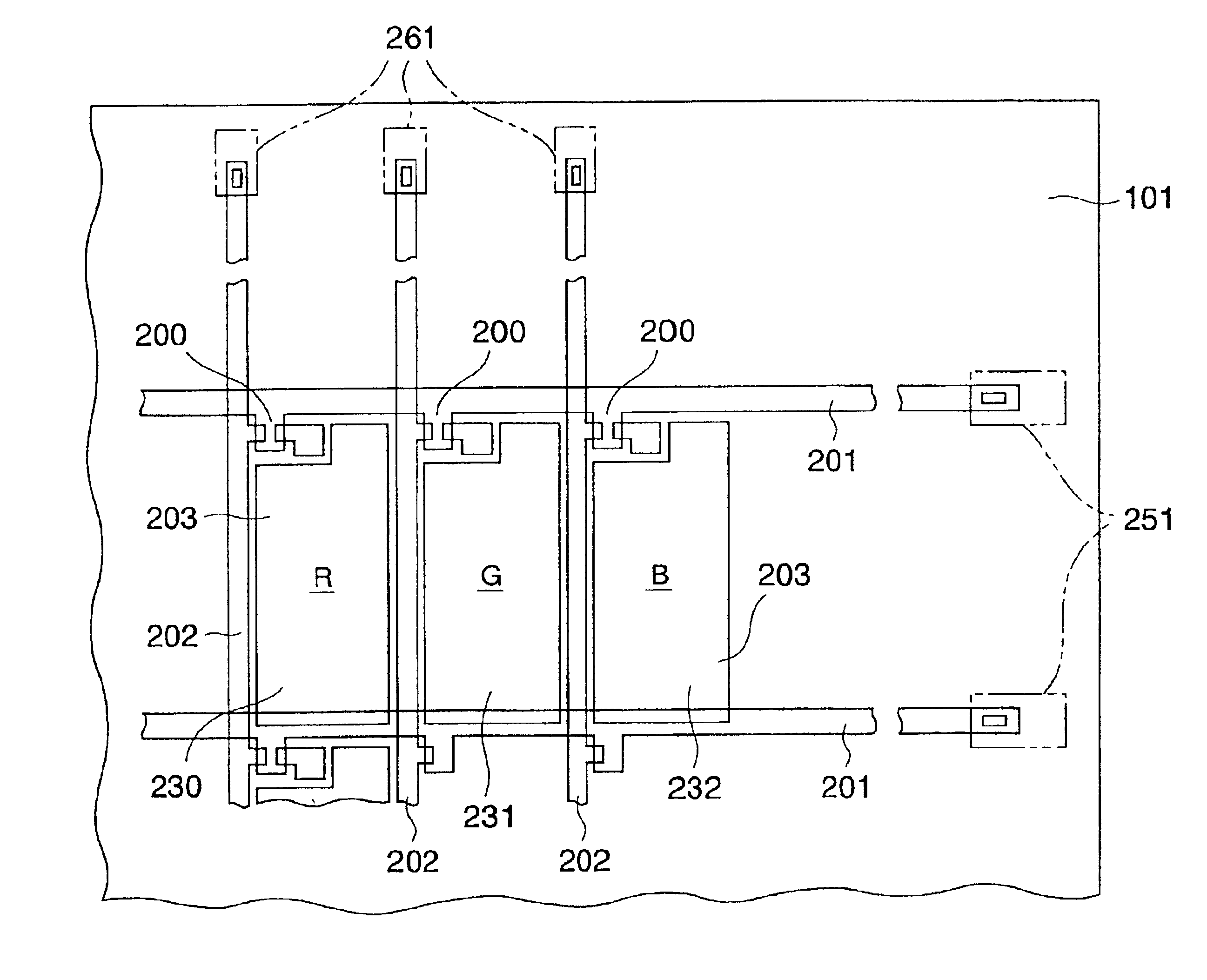
[0045]The following description will describe embodiments of the present invention in detail with reference to the accompanying drawings. To begin with, the present invention will be explained. FIG. 3 is a plan view showing a COT substrate in an active matrix type color liquid crystal display device of the present embodiment. The COT substrate includes a transparent insulating substrate 101 on which provided are a plurality of gate bus lines 201 adequately spaced apart in parallel to each other, a plurality of drain bus lines 202 adequately spaced apart in parallel to each other in such a manner as to intersect at right angles with the gate bus lines 201, pixel electrodes 203 formed in regions defined by these bus lines, and TFTs 200 provided in the vicinity of intersections of the gate bus lines 201 and drain bus lines 202.
[0046]FIGS. 4A through 4F are plan views and cross sectional views showing an arrangement of the color liquid crystal display device of the present embodiment. F...
second embodiment
[0064]The following description will describe the present invention. An overall arrangement of a COT substrate in an active matrix type color liquid crystal display device of the present embodiment is the same as the arrangement of the COT substrate shown in FIG. 1. FIGS. 11A through 11F are plan views and cross sectional views showing a construction of the color liquid crystal display device of the present embodiment. FIG. 11A is a plan view showing a region corresponding to one pixel on the active matrix substrate, FIG. 11B is a plan view showing a gate terminal portion 251, and FIG. 11C is a plan view showing a drain terminal portion 261. FIGS. 11D through 11F are cross sectional views taken along the lines AA′, BB′ and CC′ in FIGS. 11A through 11C, respectively. As shown in FIG. 11D, in a TFT 200, a gate electrode made of a Ti / Al film 102 is formed on a transparent insulating substrate 101, and a gate insulating film made of an SiN film 103 is formed on the gate electrode. A sem...
PUM
 Abstract
Description
Claims
Application Information


