Semiconductor laser device

a laser device and semiconductor technology, applied in the field of semiconductor laser devices of facet-emitting type, can solve the problems of large strain, rapid deformation of laser diodes, and catastrophic failure of this mode, and achieve the effect of good thermodynamic stability and higher reliability

Inactive Publication Date: 2005-05-24
FURUKAWA ELECTRIC CO LTD
View PDF7 Cites 10 Cited by
  • Summary
  • Abstract
  • Description
  • Claims
  • Application Information

AI Technical Summary

Benefits of technology

[0019]In a still further preferred exemplary embodiments of these aspects of the present invention, relatively thin barrier layers are located (i.e., disposed) on either side of the quantum well layer, and two optical confinement layers are located on either side of this group of layers. The inventors have discovered that the specific barrier layers substantially reduce the threshold current required for lasing, and improve the temperature dependence (behavior) of the threshold current. In preferred implementations, the barrier layers are approximately 2 nm to 10 nm in thickness, and comprise GaAs or GaAsP while the optical confinement layer comprises Al0.2Ga0.8As.
[0020]The inventors have found the GaAsSb material of the present invention to be more thermodynamically stable than the InGaAs material used in 980-nm band layers, and to exhibit less degradation over time.
[0025]Accordingly, it is an objective of the present invention to provide an active semiconductor layer which has good thermodynamic stability.
[0026]It is a further objective of the present invention to enable the construction of semiconductor laser devices which emit light at high output power of 200 mW or more in the 980-nm band and in single transverse mode, with higher reliability relative to conventional InGaAs based laser devices.
[0027]It is a still further objective of the present invention to enable the construction of such devices which can operate for longer periods of time without catastrophic optical failure as compared to conventional InGaAs based laser devices.

Problems solved by technology

The precipitate creates a localized large strain in the quantum well region due to a large mismatch.
If the strain around the precipitate exceeds a certain amount, dislocation loops appear around the precipitate, and then the laser diode degrades quickly and catastrophic failure occurs.
Thus, the catastrophic failure of this mode (long-duration degradation mode: LDDM) suddenly happens after a long period of time where no degradation is observed.
The LDDM is difficult to remove by the usual screening procedure, for example, burn-in testing.
The failure caused by the LDDM limits the lifetime of laser diodes (LDs) which use InGaAs quantum wells.

Method used


Image

  • Semiconductor laser device
  • Semiconductor laser device
  • Semiconductor laser device

Examples


Embodiment Construction

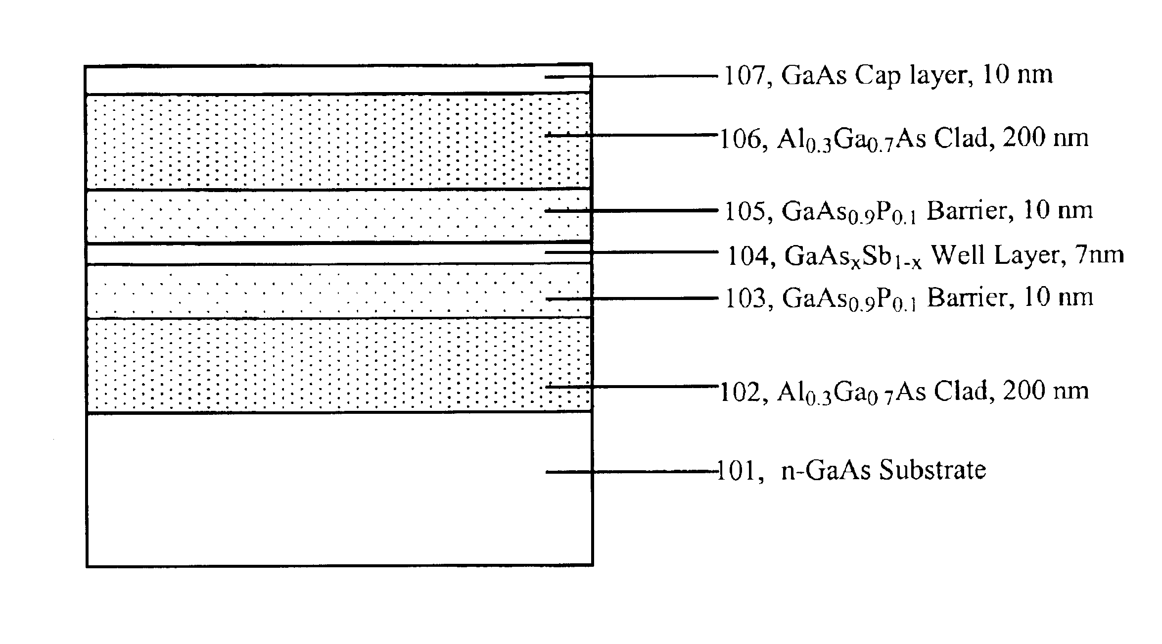
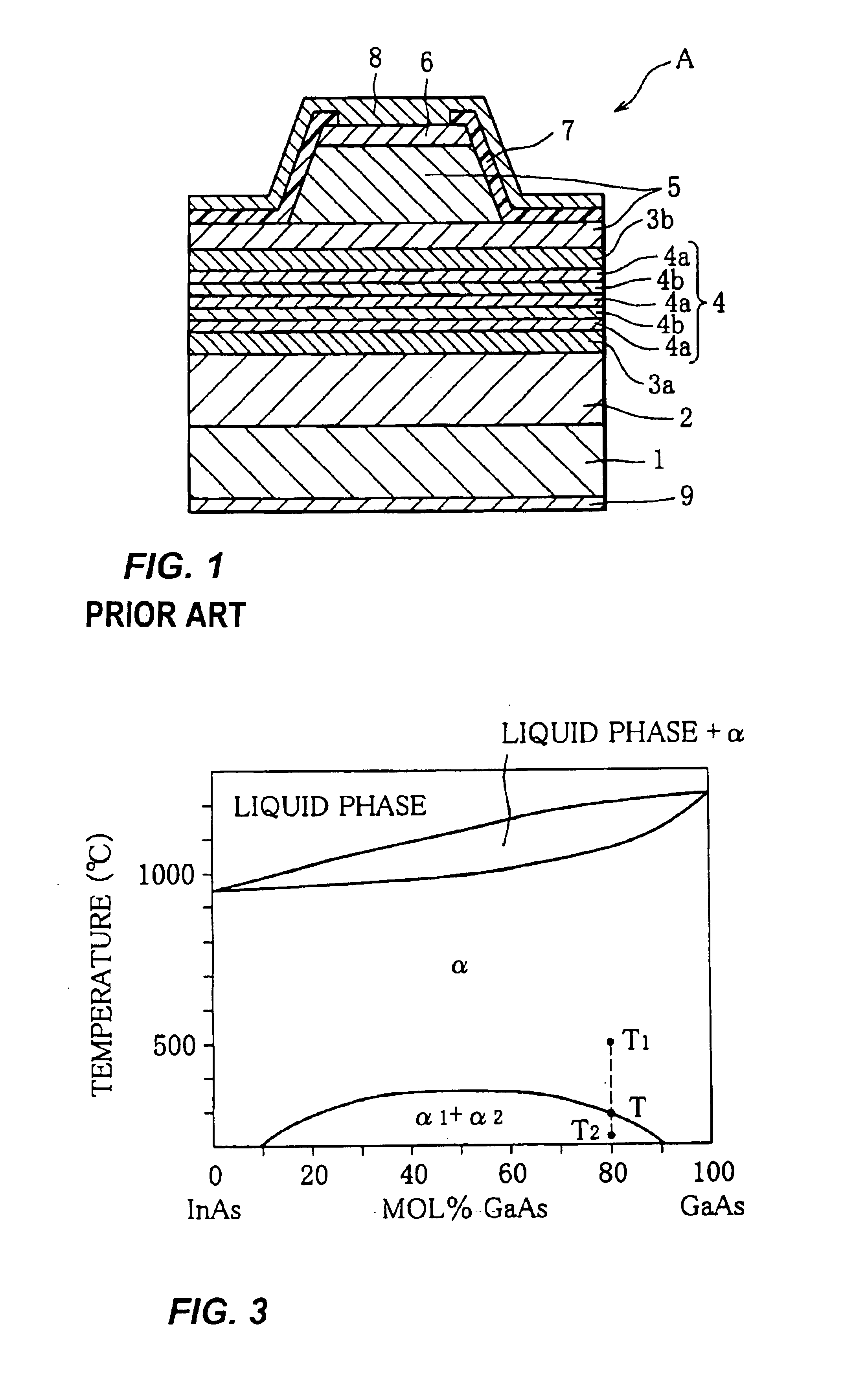
[0052]There is an increasing demand that the laser devices which emit at a wavelength band of 980 nm for EDFAs (Erbium-doped Fiber Amplifiers) should be driven to generate high optical power. In the applications where a laser device A shown in FIG. 1, for example, is driven to generate high power of 200 mW or greater over a long period of time to realize coupling to a single mode fiber (SMF), higher optical density is created.

[0053]Additionally, laser devices which emit at a wavelength band of 1050 nm are developed in order to apply for TDFAs (Thulium-doped Fiber Amplifiers). TDFAs make the available bandwidth for dense wavelength-division multiplexing (DWDM) to expand to the short wave region of 1460-1480 nm (S-band). The structure of these 1050 nm-LDs also contains InGaAs quantum wells, same as the device A.

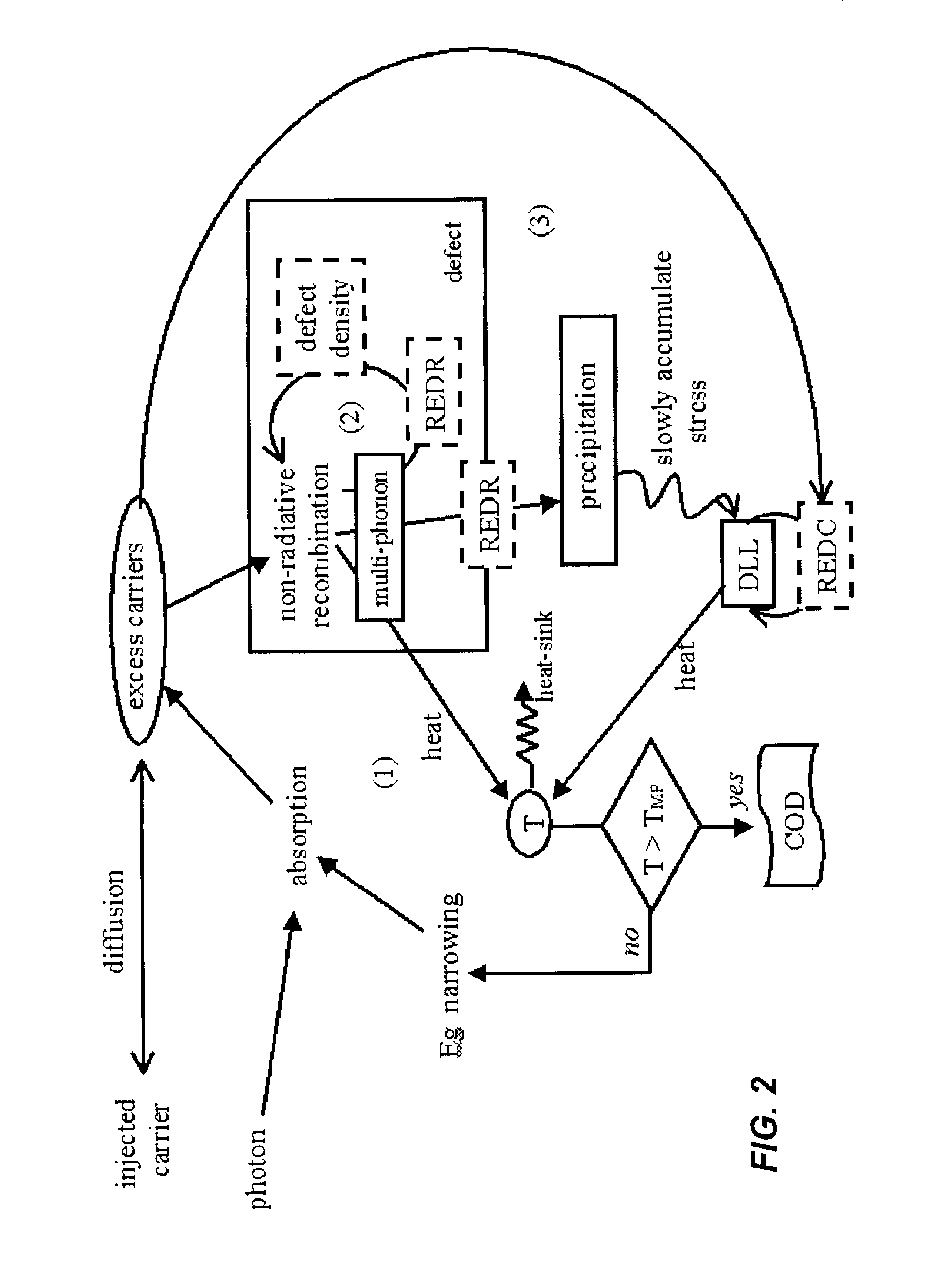
[0054]In the development of these LDs, the progress for the expansion of output power is often limited by the degradation in the higher power operations. Generally, the screeni...


PUM


Abstract

Disclosed are semiconductor laser devices which hardly have degradation when used to generate high power of 200 mW or greater over a long period of time. An exemplary semiconductor laser device comprising a semiconductor substrate, and a layer structure formed on the semiconductor substrate and having an active layer with a quantum well layer formed of a ternary system mixed crystal of a III-V compound semiconductor. The material of the quantum well layer is formed in an equilibrium phase which is thermodynamically stable at both the growth temperature and the operating temperature. The material preferably has a substantially homogeneous disordered microstructure. In a preferred embodiment, the material comprises GaAsSb. The quantum well layer exhibits improved thermodynamic stability, and the device can emit light in the 980 nm band at high power levels for longer periods of time without failure in comparison to conventional InGaAs 980 nm pumping lasers.

Description

CROSS REFERENCE TO RELATED APPLICATION[0001]This application is based on Japanese patent application 2001-251,364, filed on Aug. 22, 2001, the whole contents of which are incorporated herein by reference.FIELD OF THE INVENTION[0002]The present invention relates to a semiconductor laser device, and, more particularly, to a facet emitting type semiconductor laser device having a Fabry-Perot cavity structure.BACKGROUND OF THE INVENTION[0003]Today, most of the laser devices which emit at a wavelength band of 980 nm are made of a GaAs-based compound semiconductor material. The following describes a typical example A of such laser devices referring to FIG. 1.[0004]This laser device A is of a ridge optical waveguide having a Fabry-Perot cavity structure. The laser device A has the following layer structure.[0005]A lower cladding layer 2 of, for example, n-Al0 3Ga0.7As is laminated on a substrate 1 of n-GaAs, followed by a lower SCH layer 3a of, for example, non-doped Al0 2Ga0.8As.[0006]A b...

Claims


Application Information

Patent Timeline
Patent Type & Authority Patents(United States)
IPC IPC(8): H01S5/00H01S5/22H01S5/343H01S5/34H01S3/06H01S3/067H01S5/028
CPCB82Y20/00H01S5/22H01S3/06766H01S3/06775H01S5/0021H01S5/02284H01S5/02438H01S2304/04H01S5/0282H01S5/146H01S5/3413H01S5/34306H01S5/028H01S5/2036H01S5/02251
Inventor YOKOZEKI, MIKIHIROSAITO, KANAMEISHII, HIROTATSUIWAMI, MASAYUKI
Owner FURUKAWA ELECTRIC CO LTD
Why Eureka
Try Eureka