Overvoltage protection circuit for a power semiconductor and method for protecting a power semiconductor from over-voltages

a protection circuit and power semiconductor technology, applied in the direction of electronic switching, pulse technique, power conversion systems, etc., can solve the problem of the power semiconductor switch being destroyed, and achieve the effect of low cost, low tolerance range, and optimized operating parameters

Active Publication Date: 2016-09-15
ROBERT BOSCH GMBH
View PDF3 Cites 0 Cited by
  • Summary
  • Abstract
  • Description
  • Claims
  • Application Information

AI Technical Summary

Benefits of technology

[0009]While power semiconductor switches, depending on the area of application, are used for voltages in the range of several hundred volts, an overvoltage detector can be used in a significantly smaller voltage range as a result of the reduction of the voltage by means of the voltage divider. Such overvoltage detectors can be obtained at a significantly lower cost. In addition, components can also be used which—independently of the voltage actually applied to the power semiconductor switch—have optimized operating parameters when selecting a suitable overvoltage detector. An overvoltage detector can, for example, be selected which has a particularly low tolerance range. As a result, the response behavior of the overvoltage protection can be improved.
[0010]Furthermore, a component can be used as the overvoltage protection which has a low-level dependence on temperature. Because high thermal losses in the form of heat also occur especially when switching large capacities, the temperature fluctuations associated therewith lead to large deviations in the response behavior of conventional protection devices. By optimally selecting suitable overvoltage protection devices, this temperature dependence can be improved.
[0011]On account of the adapted response voltage of the corresponding overvoltage protection, the ageing behavior of the overvoltage protection can also furthermore be improved. Due to the reduced voltage range, overvoltage protection components can be used which age significantly less. This leads to considerably smaller safety margins being required when dimensioning the overvoltage protection device according the invention; and therefore the response behavior can be better adapted to the breakdown voltage of the power semiconductor switch being used.
[0012]In one embodiment of the overvoltage protection circuit, the overvoltage detector is a Zener diode, a suppression diode or an avalanche diode. Below a predetermined voltage, these components behave initially like a conventional diode. If the voltage applied to such a diode exceeds a predefined limit voltage in reverse direction, such a diode also becomes conductive in reverse direction. Hence, the fact that a predetermined limit voltage has been exceeded can be detected in a simple manner.
[0013]In one embodiment, the predefined voltage, at which the overvoltage detector passes into an at least partially electrically conductive state, is less than 10 volts. The predefined voltage, at which the overvoltage detector passes into the conductive state, lies approximately in the range between 5 and 6 volts. Overvoltage detectors, in particular the aforementioned Zener or suppression diodes, having a response voltage in this range can be manufactured especially cost effectively and with very good properties. Such overvoltage detectors have a particularly low tolerance requirement with regard to the response voltage. In addition, the overvoltage detectors also have a low temperature dependence for this voltage range.

Problems solved by technology

If the voltage between the terminals of the power semiconductor switch rises above said breakdown voltage, there is then the danger of the power semiconductor switch being destroyed.
Such a controller has, however, low dynamics so that short overvoltage spikes cannot be compensated by the same, whereby the use of the previously described Zener or suppression diodes becomes necessary.

Method used


Image

  • Overvoltage protection circuit for a power semiconductor and method for protecting a power semiconductor from over-voltages
  • Overvoltage protection circuit for a power semiconductor and method for protecting a power semiconductor from over-voltages
  • Overvoltage protection circuit for a power semiconductor and method for protecting a power semiconductor from over-voltages

Examples


Embodiment Construction

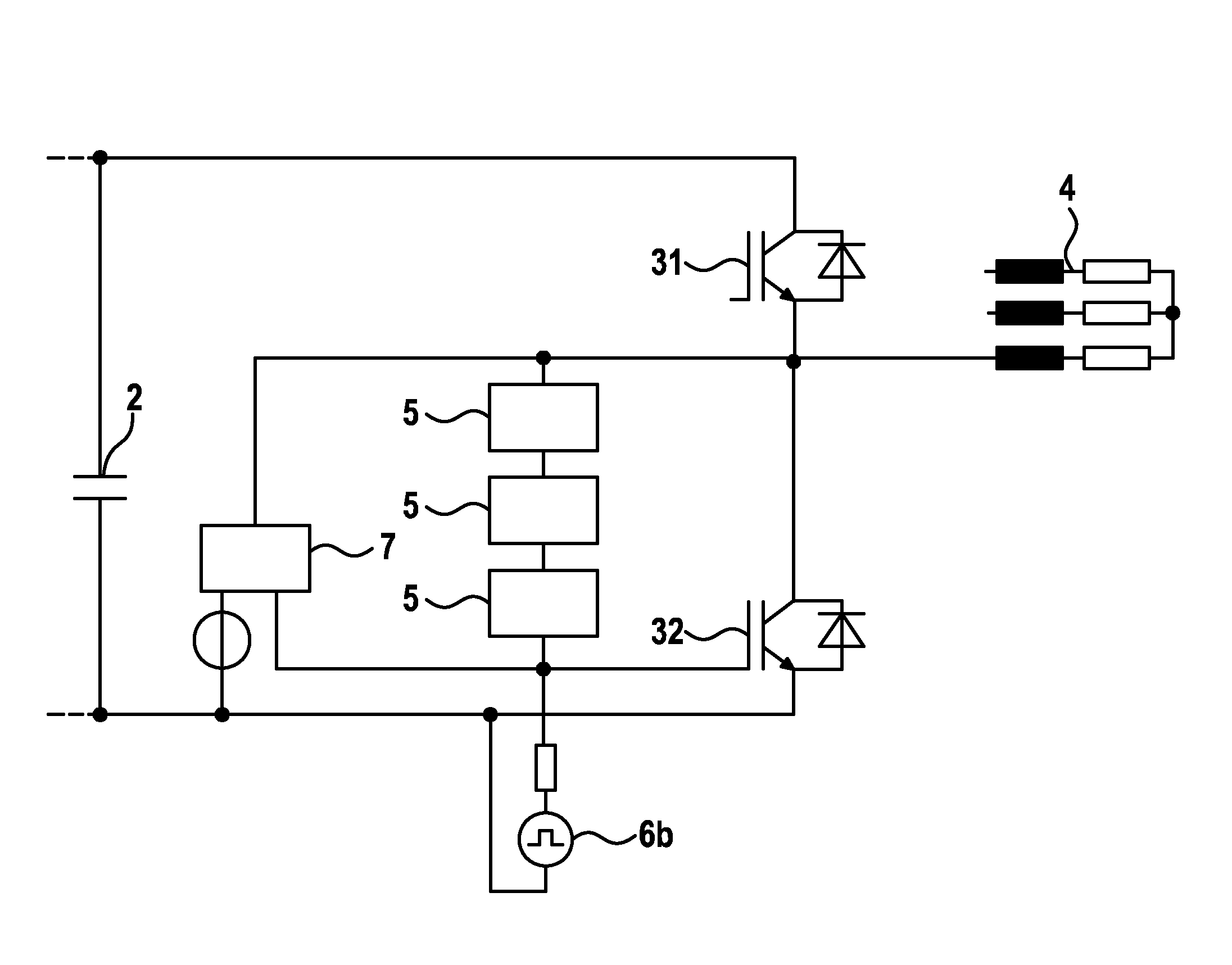
[0029]FIG. 1 shows a basic circuit diagram of a three-phase inverter for a drive system. A DC voltage is initially provided by an electrical storage unit 1, for example a battery. This DC voltage is buffered by a DC-link capacitor 2 and is subsequently supplied to an inverted rectifier 3 (inverter). The inverter 3 converts the supplied DC voltage in such a way that an AC voltage results which is suitable for activating an electrical drive 4.

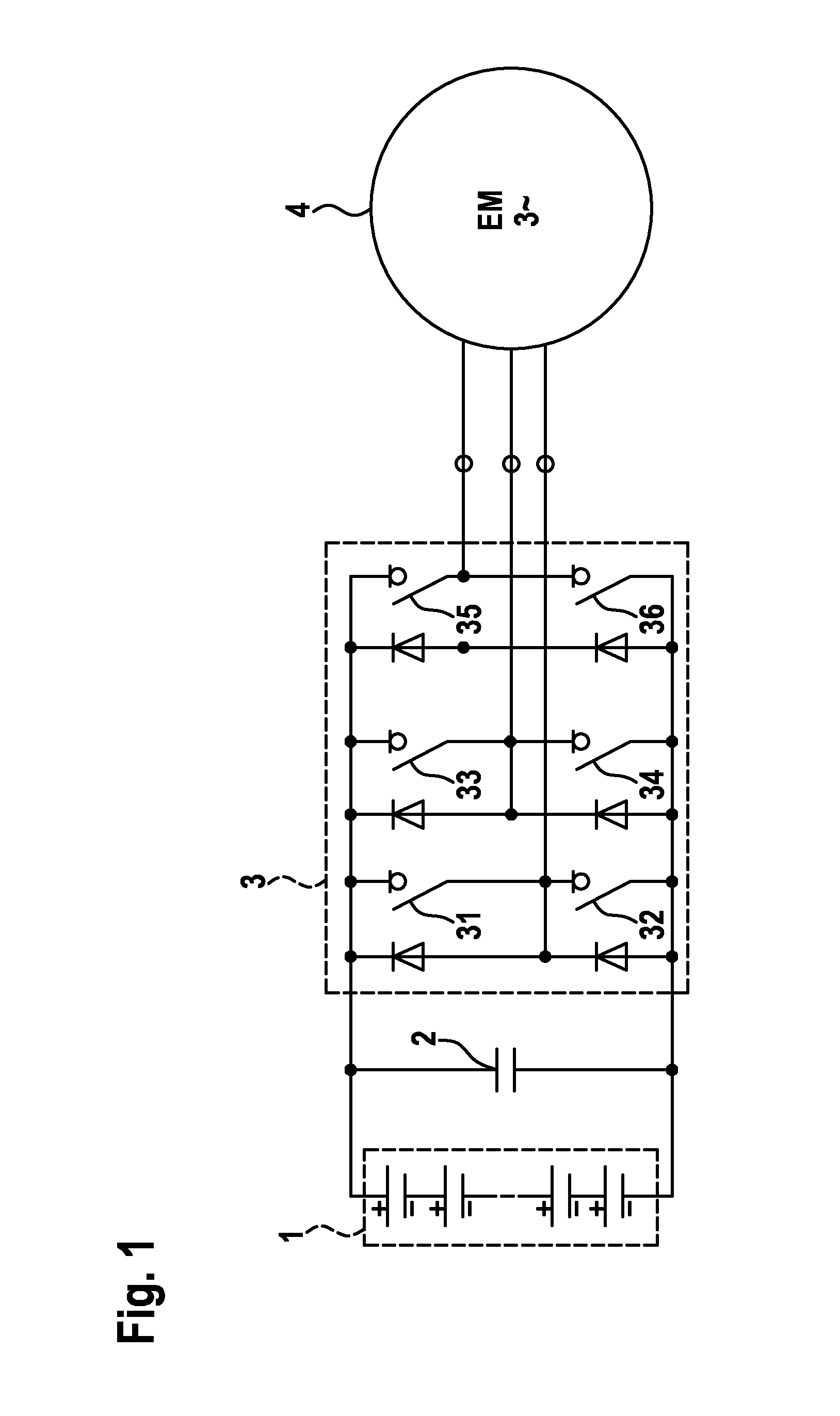
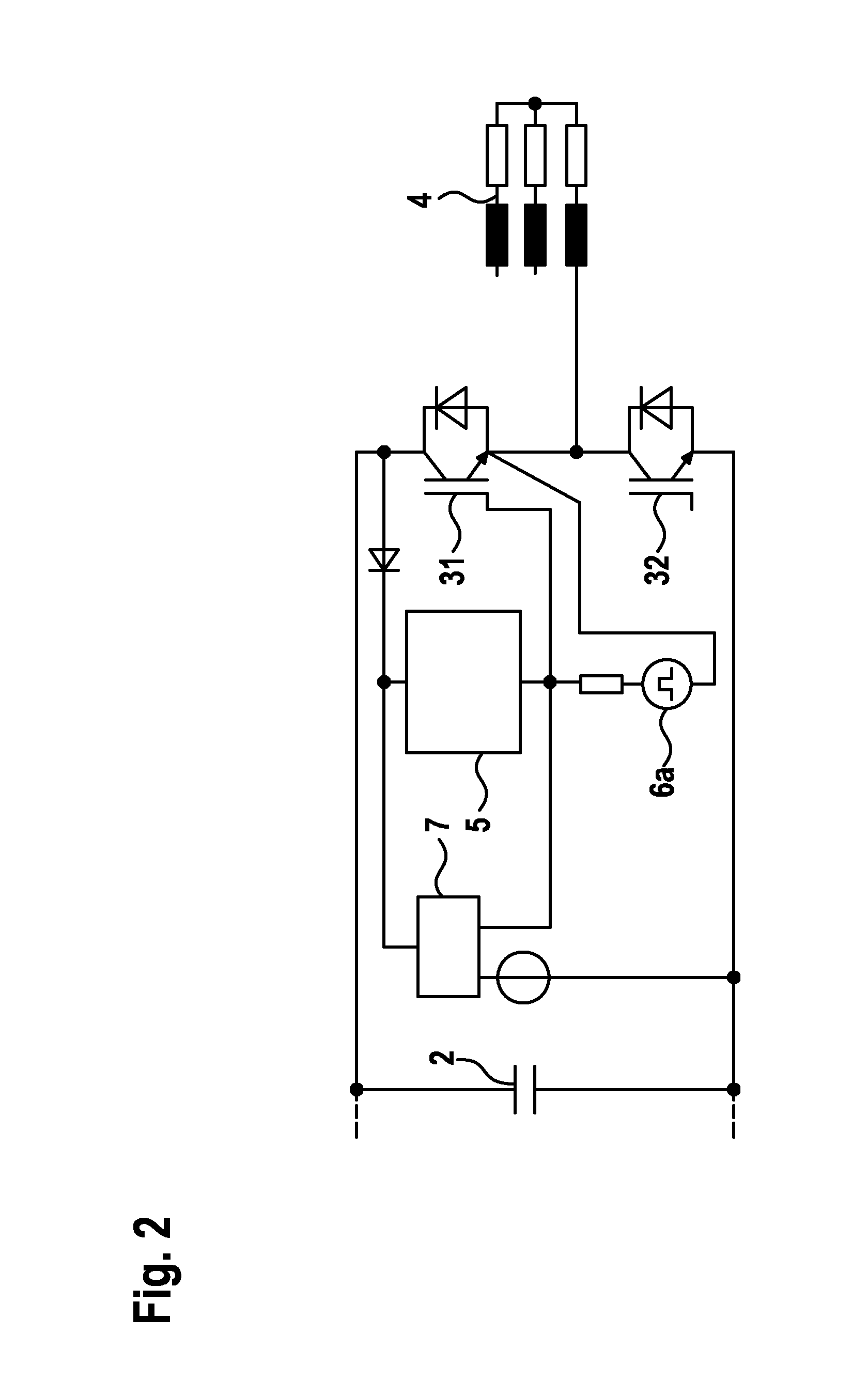
[0030]The inverter 3 comprises six power semiconductor switches 31-36 in the example depicted here. The semiconductor switches 31-36 preferably relate in each case to a MOSFET or an IGBT. In order to protect the power semiconductor switches 31-36, a free-wheeling diode is connected in each case in parallel to each of these components. The overvoltage protection circuit for each of the power semiconductor switches 31-36, which is described in greater detail below, is not depicted in this figure for the sake of clarity.

[0031]Although the present in...


PUM


Abstract

The invention relates to an overvoltage protection circuit (5) and a method for protecting a power semiconductor (31, 32) from over-voltages. For this purpose, a voltage applied across a power semiconductor switch is first converted to a lower voltage signal corresponding to the voltage applied to the power semiconductor switch by means of a resistance voltage divider. The reduced voltage signal is then evaluated by means of an overvoltage detector, such as a Zener or suppression diode, and the power semiconductor switch to be protected is activated if the response voltage of said diode is exceeded. By lowering the voltage level by means of a voltage divider, a Zener or suppression diode having a lower voltage level can be used for monitoring the overvoltage, said Zener or suppression diode having improved operating properties in comparison with corresponding diodes having a higher voltage level.

Description

BACKGROUND OF THE INVENTION[0001]The present invention relates to an overvoltage protection circuit for a power semiconductor and a method for protecting a power semiconductor from over-voltages.[0002]Power switches on the basis of semiconductor switches are known. Because such power semiconductor switches do not have any moving mechanical parts, they ensure a wear-free operation with very short switching times over a long period of time. Bipolar transistors with an insulated gate (IGBT) or metal-oxide-semiconductor field-effect transistors (MOSFET) are, for example, used as such power semiconductor switches. In order to protect these transistors, the power semiconductor switches are additionally equipped with a free-wheeling diode. Because the dielectric strength of such power semiconductor switches is limited, additional circuit means have to be in place in order to ensure that the voltage between input and output of the power semiconductor switch is always less than a so-called b...

Claims


Application Information

Patent Timeline
Patent Type & Authority Applications(United States)
IPC IPC(8): H03K17/56H02M1/32H02H9/04
CPCH03K17/56H02M1/32H02H9/044H03K17/0828
Inventor PURCAREA, CALINFEUERSTACK, PETER
Owner ROBERT BOSCH GMBH
Why Eureka
Try Eureka