High gain detector amplifier with enhanced dynamic range for single photon read-out of photodetectors

a detector amplifier and high gain technology, applied in the field of ultralow noise photon detection, can solve the problem of large margin of video signal over background noise of camera electronics, and achieve the effect of generating minimum fixed pattern noise, facilitating single-photon read-out, and ultra-low nois

Inactive Publication Date: 2005-05-31
SAMSUNG ELECTRONICS CO LTD
View PDF30 Cites 35 Cited by
  • Summary
  • Abstract
  • Description
  • Claims
  • Application Information

AI Technical Summary

Benefits of technology

[0013]In general, the present invention provides an ultra-low noise, high-gain pixel amplifier to facilitate single-photon read-out across the electromagnetic spectrum from the x-ray to long IR bands at video frame rates and higher. The present invention supports various types of high impedance detectors, both photovoltaic and photoconductive, and generates minimum fixed pattern noise.
[0014]More particularly, the present invention is an adaptive detector amplifier circuit comprising a high-gain detector interface with self-nulling offset suppression to simultaneously provide high gain, low offset non-uniformity and wide dynamic range. The front-end provides both high gain and wide signal bandwidth by integrating the photocharge on the detector's capacitance. The front-end also facilitates extremely low read noise by using a feedback-enhanced reset amplifier to suppress the kTC noise below 1 e−. The integrating photocharge modulates a current source whose gain-proportioned signal may be integrated during the entire integration time or for only a fraction of the integration time, at the operator's choice. This gain is adjustable, varying exponentially with gain voltage and can be set appropriately larger at small signal levels to enable sub-electron read noise even in the presence of the kTC noise of the integration capacitor.
[0015]Since the current required for high gain will be large and since variations in the threshold voltage of the modulated transistor would normally generate large non-uniformity in these large currents, the present invention incorporates an adaptive skimming circuit at the back-end to minimize the signal non-uniformity. Though the present circuit can be readily configured as an integrator with a rolling-type electronic shutter, synchronous image formation (snapshot) is facilitated by appropriately applying a global reset clock rather than a rastered reset clock. This function separates signal integration on the diode from the gain-proportioned assimilation on an integration capacitor, Cint. This requires the gain to be set high enough to allow the charging of Cint in a small fraction of the frame time. If desired, a more conventional snapshot circuit with a second integration capacitor can also be employed. Additionally, one embodiment of the present invention includes a source-follower amplifier at the pixel's output to buffer the signal read through the bus. This amplifier may not be necessary if the charge integrated in the cell is large enough.
[0016]The present solution can be integrated into the typical pixel pitches normally used for single-photon detection (from 40 μm to 125 μm) to amplify only the noise-free photo-generated signal for subsequent processing or display. The resulting video signal has large margin over the background noise of the camera electronics even at very low levels of ambient light without need for supplementary illumination.

Problems solved by technology

The resulting video signal has large margin over the background noise of the camera electronics even at very low levels of ambient light without need for supplementary illumination.

Method used


Image

  • High gain detector amplifier with enhanced dynamic range for single photon read-out of photodetectors
  • High gain detector amplifier with enhanced dynamic range for single photon read-out of photodetectors
  • High gain detector amplifier with enhanced dynamic range for single photon read-out of photodetectors

Examples


Embodiment Construction

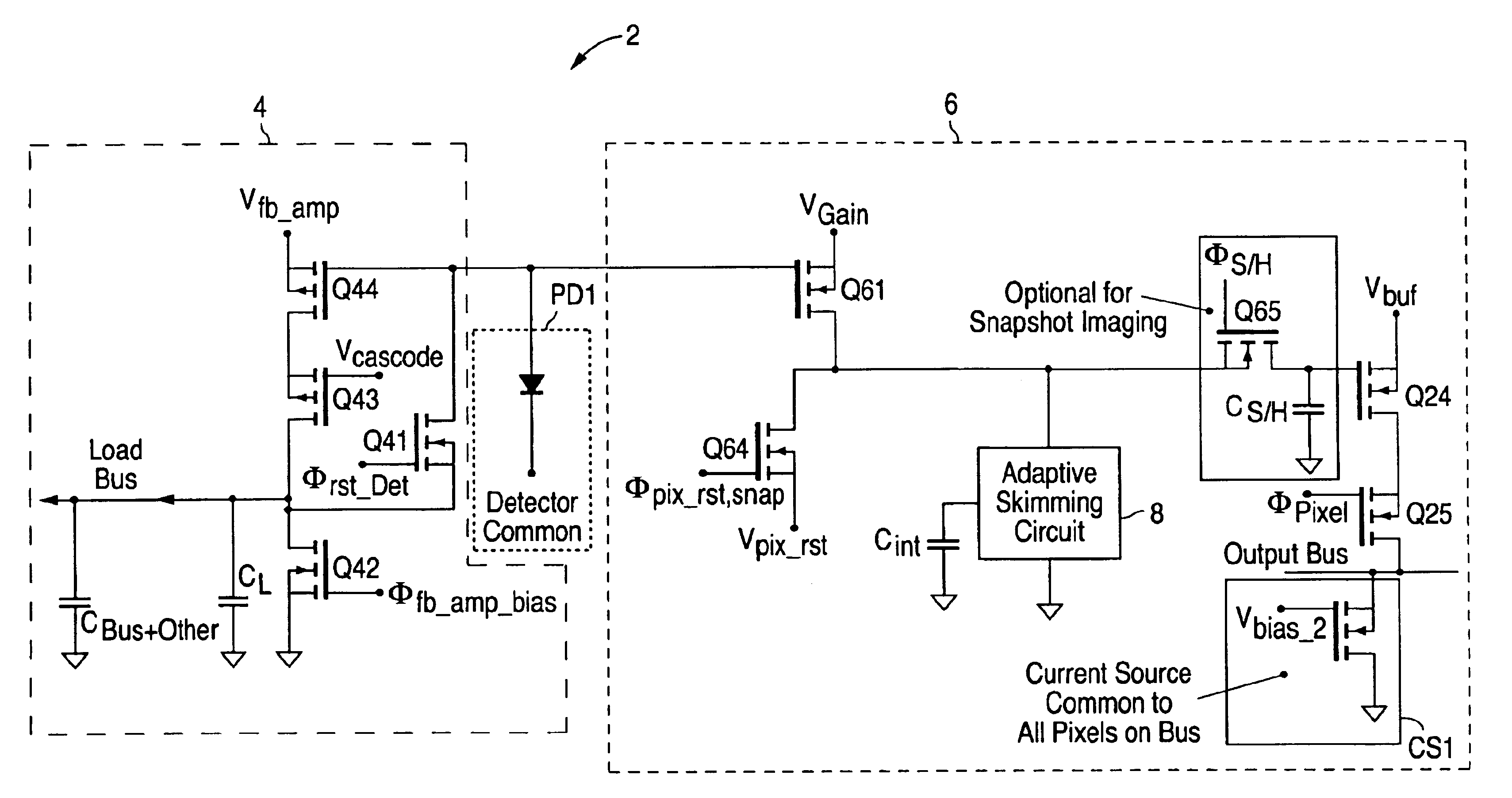
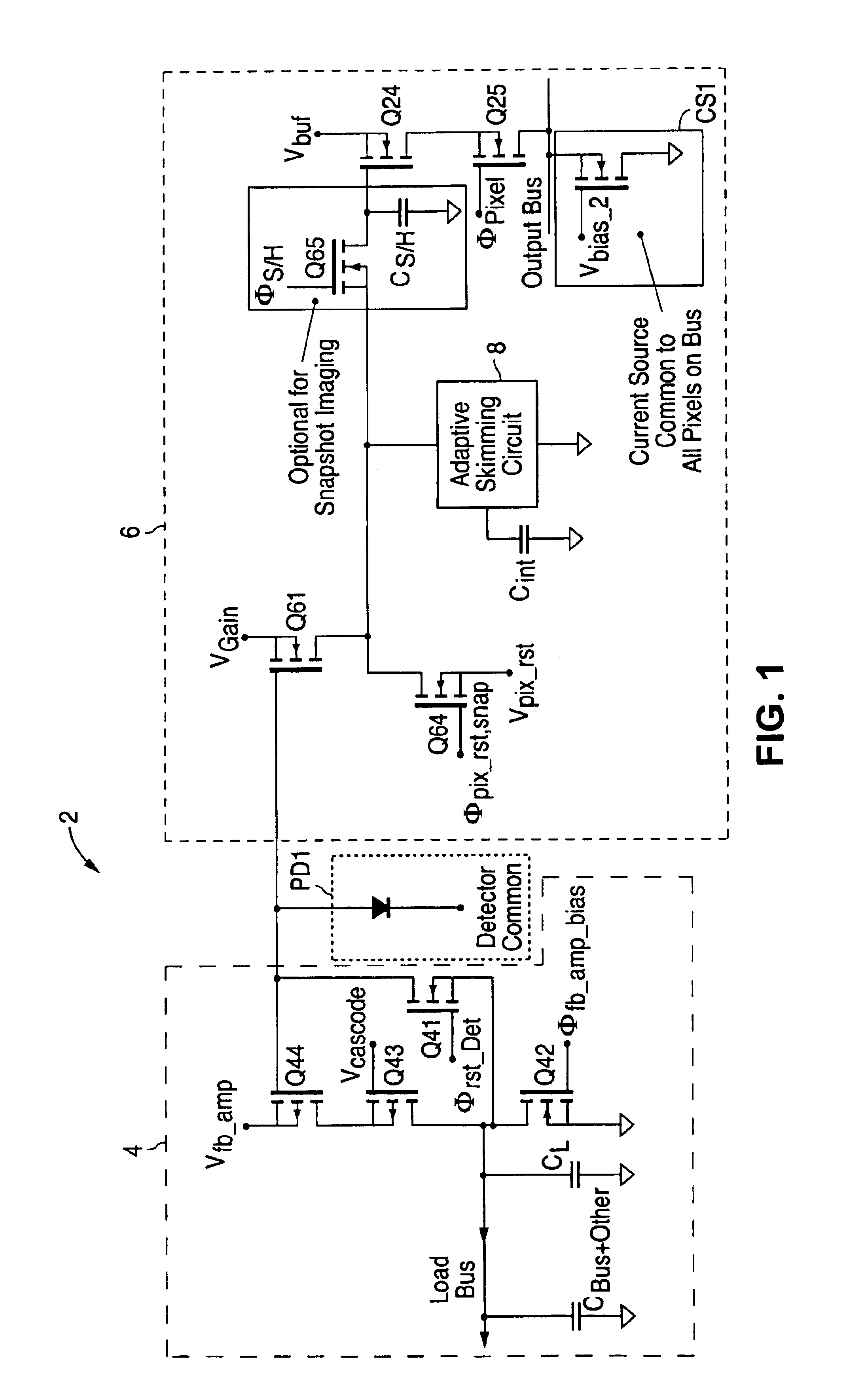
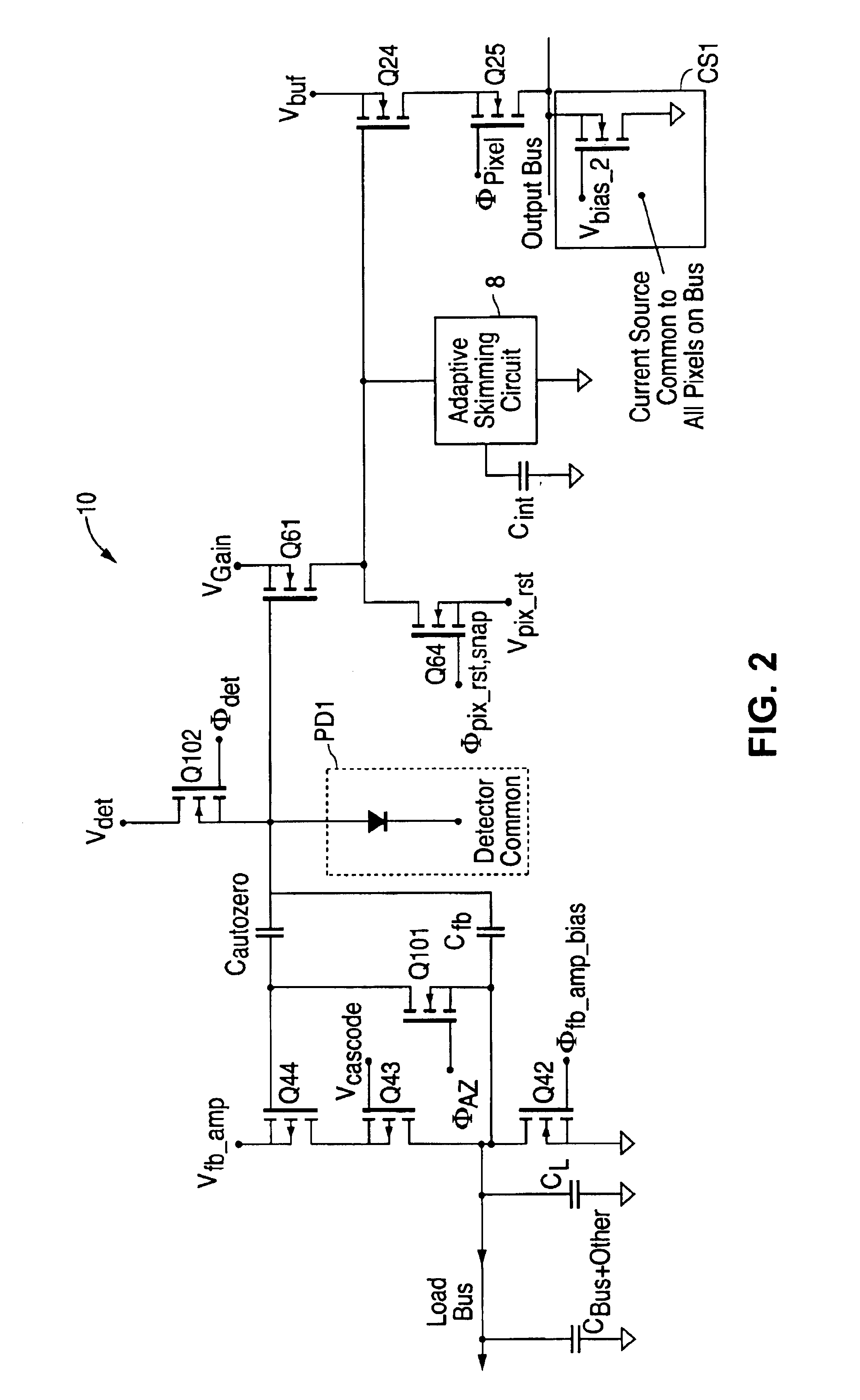
[0022]The following description is provided to enable any person skilled in the art to make and use the invention and sets forth the best modes contemplated by the inventors for carrying out the invention. Various modifications, however, will remain readily apparent to those skilled in the art, since the basic principles of the present invention have been defined herein specifically to provide a low-noise, high-gain, wide dynamic range pixel amplifier with high bandwidth for single photon readout of various photodetectors in imaging arrays. Any and all such modifications, equivalents and alternatives are intended to fall within the spirit and scope of the present invention.

[0023]The present invention provides a high bandwidth, ultra low-noise pixel amplifier that is capable of single photon read-out of photodetectors in extremely low-light conditions, i.e. photon flux levels approaching zero photons per sampling period. This circuit can be used to effectively count incident photons ...


PUM


Abstract

An ultra-low noise, high gain interface pixel amplifier is provided with capability for single-photon readout of standard photodetectors at high electrical bandwidths for diverse spectral bandpass from the x-ray to long IR bands. The detector charge modulates a source follower whose output is double sampled to remove correlated noise by a compact stage that also provides optimum level shift for subsequent amplification of the full signal excursion. The level-shifted signal finally drives a compact amplifier that generates a robust end-to-end transimpedance. Single-photon readout of photodetectors at high electrical bandwidths in small pixel areas is thereby facilitated.

Description

[0001]The present application is related to U.S. patent application Ser. 09 / 675,278 entitled “SELF-ADJUSTING ADAPTIVE MINIMAL NOISE INPUT AMPLIFIER”, filed Sep. 29, 2000; and is also related to U.S. Pat. No. 6,504,141, entitled “ADAPTIVE AMPLIFIER CIRCUIT WITH ENHANCED DYNAMIC RANGE”, filed Sep. 29, 2000; the disclosures of which are herein incorporated by reference.BACKGROUND OF THE INVENTION[0002]1. Field of the Invention[0003]This invention relates to ultra-low noise photon detection in low-light-level conditions and, specifically, to low-noise, high-gain, wide dynamic range pixel amplifiers with high bandwidth for single photon readout of various photodetectors in imaging arrays.[0004]2. Description of the Related Art[0005]Optical sensors transform incident radiant signals in the X-ray (λ<0.00 μm), ultraviolet (λ=0.001-0.4 μm), visible (λ=0.4-0.8 μm), near infrared (IR) (λ=0.8-2 μm), shortwave IR (λ=2.0-2.5 μm), mid IR (λ=2.5-5 μm), and long IR (λ=5-20 μm) bands into electric...

Claims


Application Information

Patent Timeline
Patent Type & Authority Patents(United States)
IPC IPC(8): H04N3/14H04N5/335H03F3/08H04N5/355H04N5/363H04N5/365H04N5/3745H04N5/378
CPCH03F3/082H04N5/3745H04N5/3651H04N5/363H04N25/65H04N25/671H04N25/77
Inventor KOZLOWSKI, LESTER J.TENNANT, WILLIAM E.
Owner SAMSUNG ELECTRONICS CO LTD
Why Eureka
Try Eureka