Semiconductor memory having hierarchical bit line structure
- Summary
- Abstract
- Description
- Claims
- Application Information
AI Technical Summary
Benefits of technology
Problems solved by technology
Method used
Image

Examples
Embodiment Construction
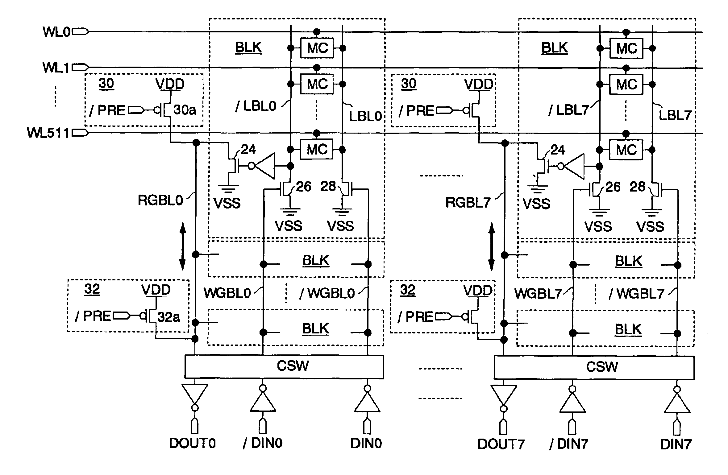
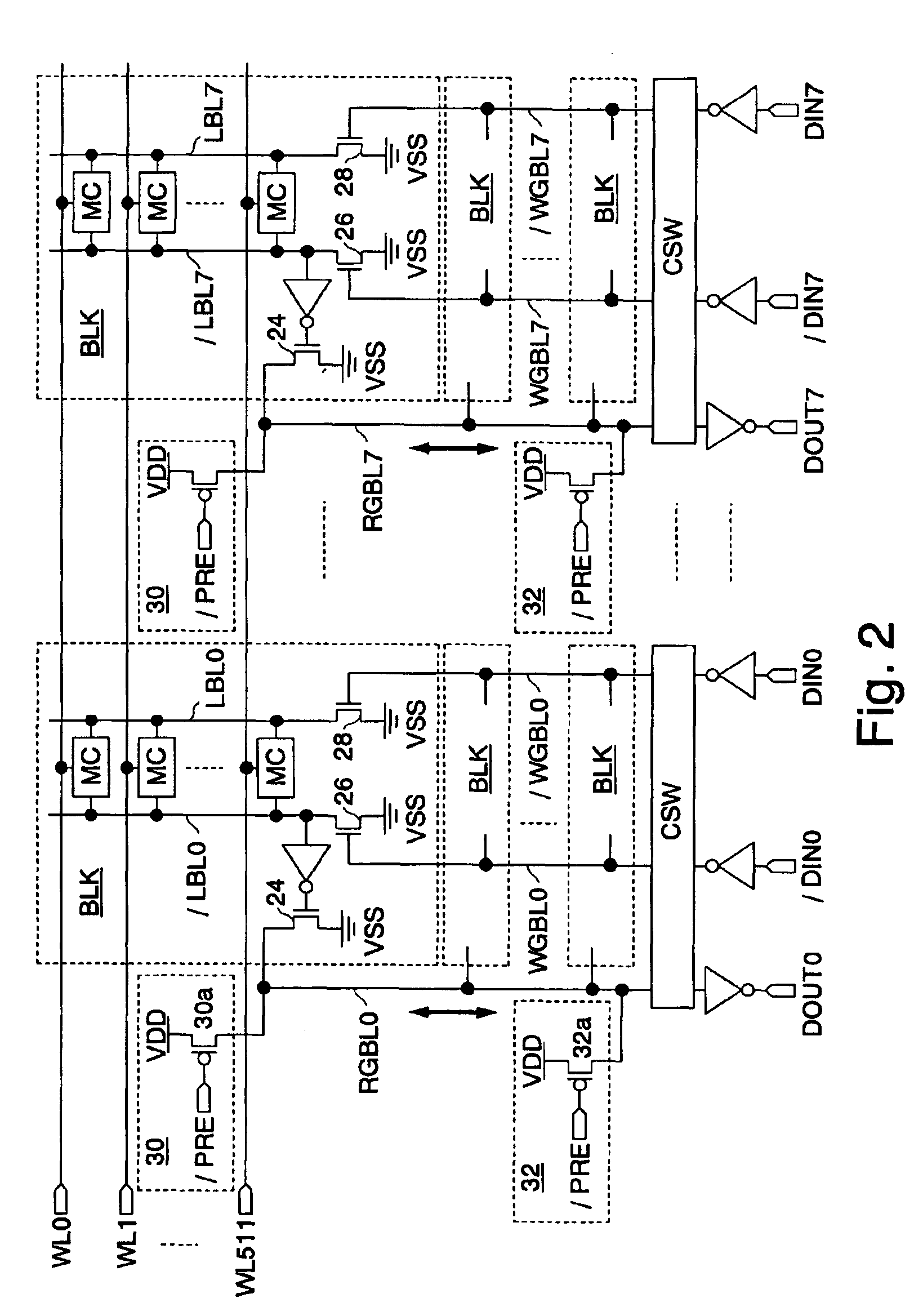
[0033]Hereinafter, embodiments of the present invention will be described with reference to the drawings. In the drawings, each thick line represents a signal line that consists of a plurality of lines. Signals with a leading “ / ” are of negative logic. Double circles in the drawings represent external terminals. In the following description, signal names may be abbreviated like a “ / CS signal” for a “chip select signal”.
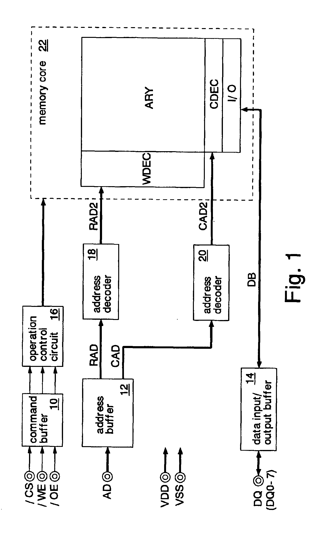
[0034]FIG. 1 shows a first embodiment of the semiconductor memory of the present invention. This semiconductor memory is formed as an SRAM on a silicon substrate by using CMOS processes.
[0035]The SRAM has a command buffer 10, an address buffer 12, a data input / output buffer 14, an operation control circuit 16, address decoders 18 and 20, and a memory core 22.
[0036]The command buffer 10 receives command signals (a chip select signal / CS, a write enable signal / WE, and an output enable signal / OE) from exterior. The address buffer 12 receives an address signal AD throug...
PUM
 Abstract
Description
Claims
Application Information
 - R&D Engineer
- R&D Manager
- IP Professional
- Industry Leading Data Capabilities
- Powerful AI technology
- Patent DNA Extraction
Browse by: Latest US Patents, China's latest patents, Technical Efficacy Thesaurus, Application Domain, Technology Topic.
© 2024 PatSnap. All rights reserved.Legal|Privacy policy|Modern Slavery Act Transparency Statement|Sitemap