
Integrated circuit with CPU and FPGA for reserved instructions execution with configuration diagnosis

a technology of integrated circuits and reserved instructions, applied in the direction of computation using denominational number representation, pulse techniques, instruments, etc., can solve the problems of inflexible response to the necessary circuits, process suspension, and inability to take advantage of fpga characteristics, so as to improve processing ability and improve processing ability

Inactive Publication Date: 2005-05-31
PANASONIC CORP
View PDF11 Cites 70 Cited by
  • Summary
  • Abstract
  • Description
  • Claims
  • Application Information

AI Technical Summary

Benefits of technology

[0009]An object of the present invention is to provide a semiconductor integrated circuit that has a CPU and an embedded FPGA, which has a high processing ability and can automatically and dynamically change circuits composed in the FPGA.

Problems solved by technology

However; in the above-mentioned conventional semiconductor integrated circuit that has a CPU and an embedded FPGA, there is a problem in which, in a case where instruction to be processed by FPGA is provided, if a circuit for executing such a processing is not composed in the FPGA, it is handled as undefined operation and the process is suspended.
In addition, in the above-mentioned conventional semiconductor integrated circuit that has a CPU and an embedded FPGA, in a case where the circuit composed in the FPGA is fixed, it does not take advantage of the FPGA characteristics in which the circuit configuration is changed dynamically and it cannot respond flexibly to the necessary circuits on each occasion.
Thus, there were limits to the processing ability improvement.
Furthermore, if the circuits composed in the FPGA are changed dynamically, it is necessary for users to designate the timing of circuit configuration change beforehand, and changes in circuit configuration cannot be executed automatically.
In other words, in a case of conventional semiconductor integrated circuits that has a CPU and an embedded FPGA, there is a problem in which processing ability improvement based on FPGA is not able to be executed automatically.

Method used


Image

  • Integrated circuit with CPU and FPGA for reserved instructions execution with configuration diagnosis
  • Integrated circuit with CPU and FPGA for reserved instructions execution with configuration diagnosis
  • Integrated circuit with CPU and FPGA for reserved instructions execution with configuration diagnosis

Examples


first embodiment

(First Embodiment)

Outline of Configuration of System

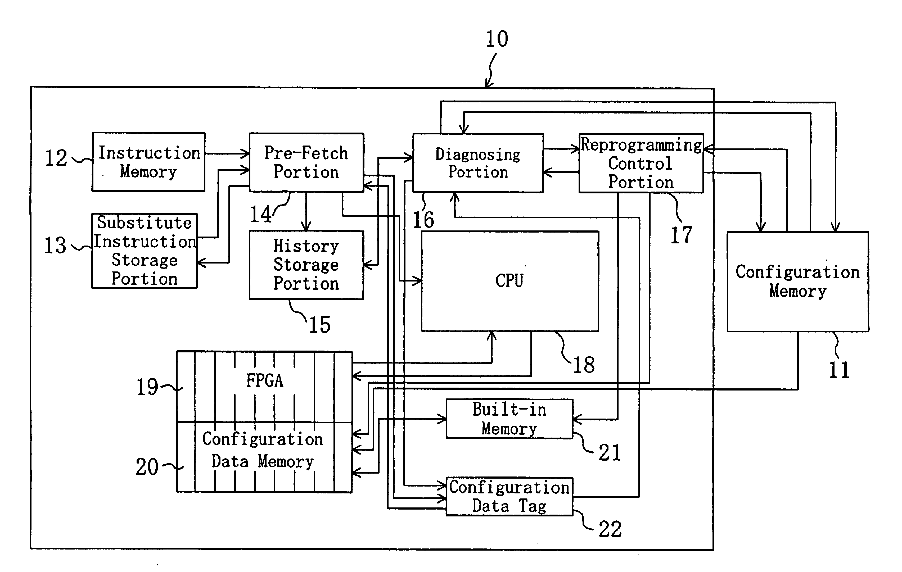
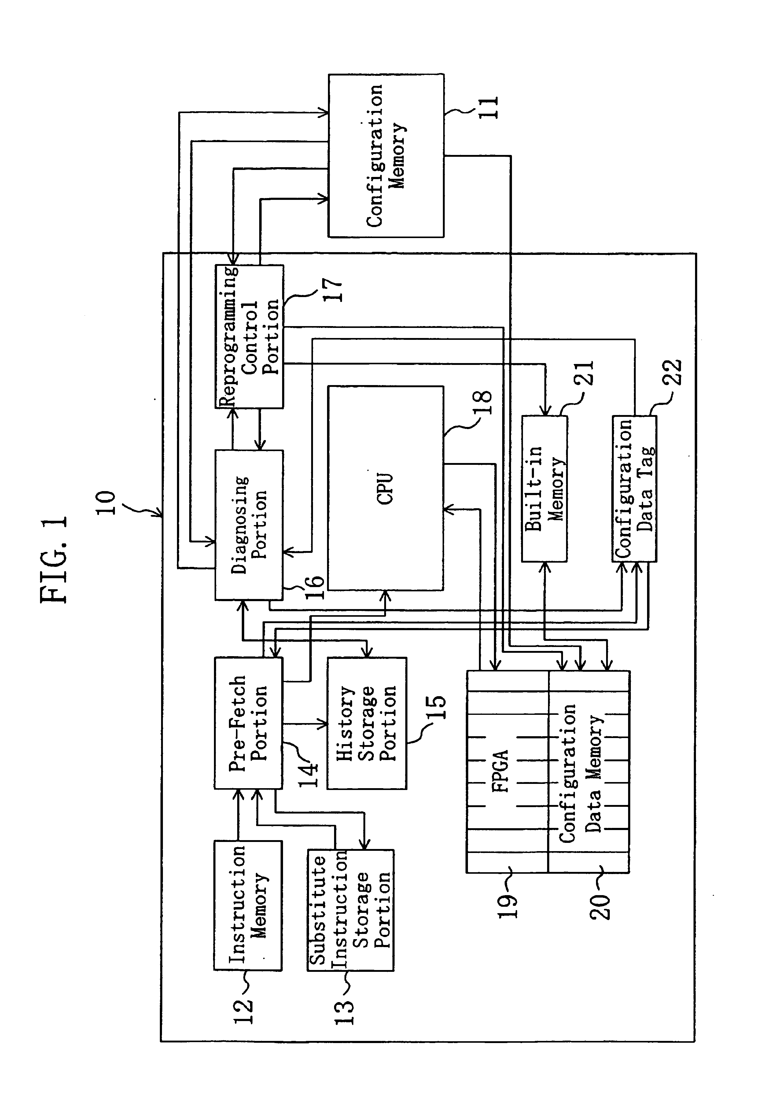
[0040]FIG. 1 is a block circuit diagram of a semiconductor integrated circuit according to a first embodiment of the present invention. As shown in the drawing, the semiconductor integrated circuit 10 of the present embodiment can send and receive signals with a configuration memory 11 provided outside. Furthermore, the semiconductor integrated circuit 10 is provided therein with an instruction memory 12 that stores the program for processing data, etc., a substitute instruction storage portion 13 that stores substitution instruction for executing by the CPU 18 a substantially equivalent processing to a reserved instruction (hereinafter referred to as the “F instruction”) processed in the FPGA 19, a pre-fetch portion 14 for fetching instructions from the instruction memory 12 and the substitute instruction storage portion 13, a history storage portion 15 for storing the history of F instruction input from the instruction memory 12,...

second embodiment

(Second Embodiment)

[0070]Next, an explanation is given on a second embodiment related to a control method where instruction memory having data configuration in which both F instruction and substitute instruction are described is provided. In the present embodiment, in the configuration shown in FIG. 1, not being equipped with substitute instruction storage portion 13 is the prerequisite.

[0071]FIG. 7 is a drawing that shows a concrete example of the case in which both F instruction and substitute instruction are described in the program of the instruction memory 12. In FIG. 7, a case in which F instruction shown in FIG. 6A, F instruction shown in FIG. 6B, and their substitute instructions are described, is taken up as examples.

[0072]As shown in FIG. 7, in a case where the F instructions are processed by embedded FPGA 19 upon receipt of the F instruction at the pre-fetch portion 14, the F instructions are sent to the CPU 18, an then, the pre-fetch portion will jump to the address addr...

third embodiment

(Third Embodiment)

[0076]In the aforementioned first and second embodiments, the F instruction is included in the program in the instruction memory, and is composed so that diagnosis of whether processing of F instruction will be executed by FPGA or not is made by detecting such F instructions. Therefore, in a case with programs that do not utilize F instructions, improvement in processing ability based on FPGA cannot be achieved since processing utilizing embedded FPGA cannot be made. Thus, in the present embodiment, program that does not use F instruction is stored in the instruction memory and processing utilizing FPGA is realized, thereby making it possible to achieve improvement in processing ability even in such a case.

[0077]FIG. 11 is a block circuit diagram of a semiconductor integrated circuit in the present embodiment. As shown in the drawing, in the present embodiment, no substitute instruction storage portion is provided. In the present embodiment, in the program inside t...


PUM


Abstract

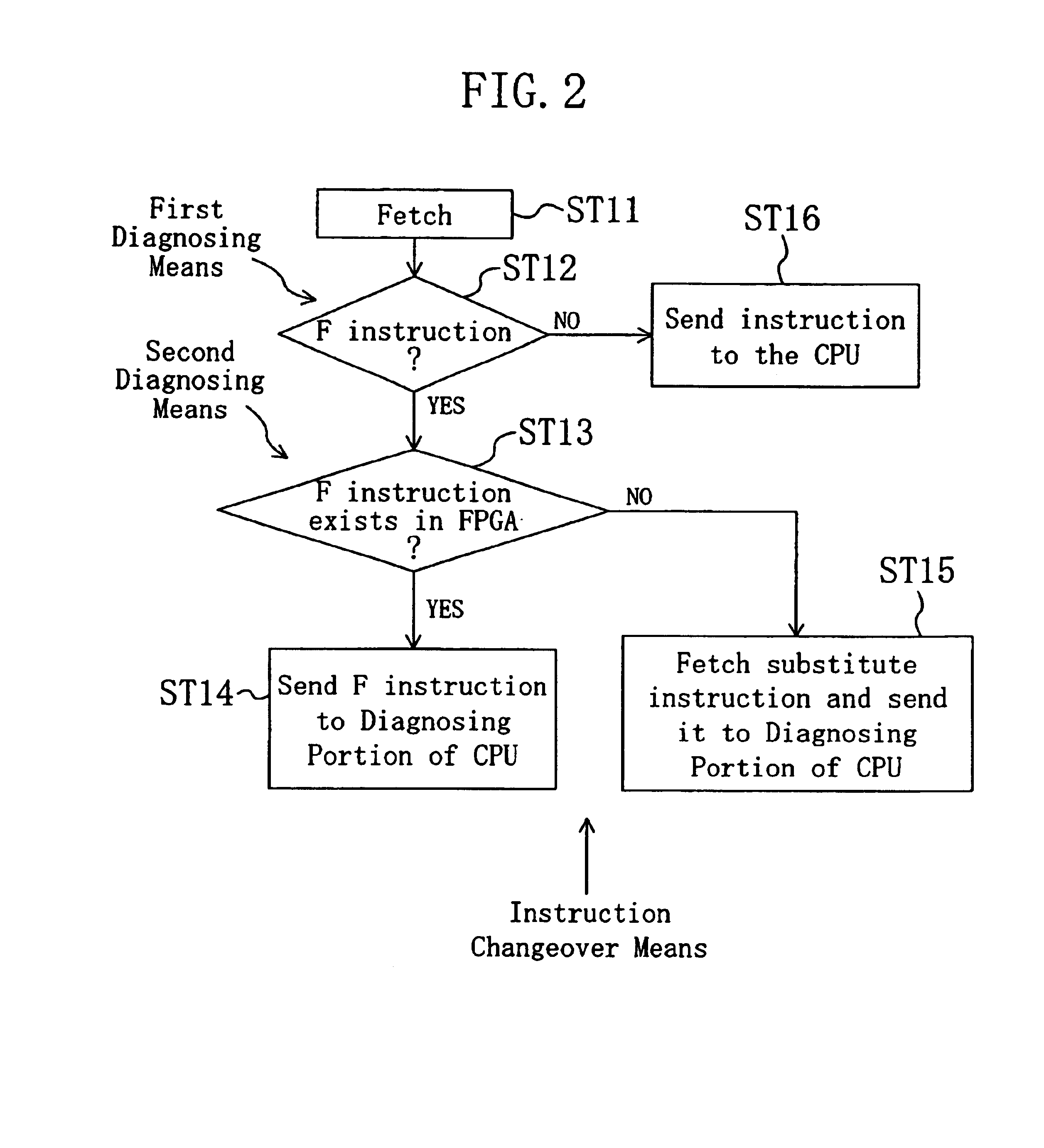
A semiconductor integrated circuits can send and receive signals to and form a configuration memory. The semiconductor integrated circuits is provided therein wiht an instruction memory, an instruction storage portion that stores reserved instructions as F instructions, and stores the substantially equivalent processing contents to the F instructions as substitute instructions for processing by the CPU, a pre-fetch portion, a history storage portion, a diagnosing portion for diagnosing the types of instructions, a reprogramming control portion for reprogramming the instructions, a CPU, an FPGA, a configuration data memory, a built-in memory, and a configuration data tag. When the configuration data of the F instruction does not exist in the FPGA, the substantially equivalent processing by FPGA is executed by the CPU by making use of the substitute instructions.

Description

BACKGROUND OF THE INVENTION[0001]This invention relates to a semiconductor integrated circuit that has a CPU and an embedded programmable device, and in particular, it relates to measures for improvement in processing ability.[0002]Programmable devices referred to as PLD (Programmable Logic Device) or FPGA (Field Programmable Gate Array) are widely known (hereinafter referred to as FPGA in this specification). FPGA is a device that enables the user to program its circuit configuration, and has a merit in which the circuit designed by the user is composed immediately to realize the operation. Especially in case of FPGA where circuit configuration is repeatedly recomposed, it also has a merit of improving the processing ability by flexibly changing the necessary circuit configuration on each occasion.[0003]Furthermore, in recent years, it has been proposed to embed the FPGA and CPU into a single semiconductor integrated circuit. In such a semiconductor integrated circuit, in addition ...

Claims


Application Information

Patent Timeline
Patent Type & Authority Patents(United States)
IPC IPC(8): G06F9/38G06F9/318G06F9/30G06F11/00G06F15/78H01L21/822H01L27/04
CPCG06F9/3017G06F9/3897G06F9/3877G06F9/30181
Inventor YANO, JUNICHIYOSHIDA, HISATOAIBA, KIMIHIKOIMAMURA, KATSUYUKIMORI, JUNICHIYAMAMOTO, JUNYA
Owner PANASONIC CORP
Learn More