

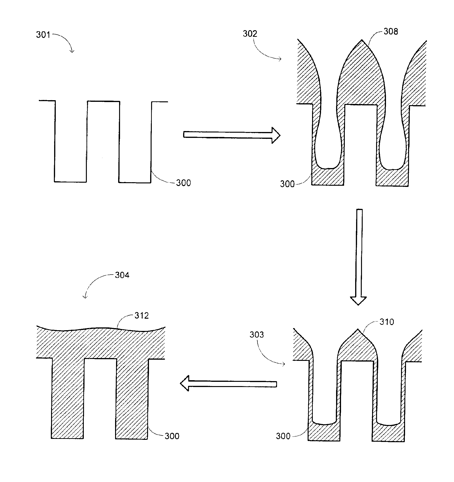
In-situ-etch-assisted HDP deposition using SiF4 and hydrogen
a technology of in-situ etching and hdp deposition, which is applied in the direction of coating, chemical vapor deposition coating, metallic material coating process, etc., can solve the problems of affecting device operation and unable to completely fill the vacuum chamber of the semiconductor manufacturer, and achieve good gapfill characteristics and reduce fluorine concentration
- Summary
- Abstract
- Description
- Claims
- Application Information
AI Technical Summary
Benefits of technology
Problems solved by technology
Method used
Image

Examples
example 1
[0068]To illustrate the gapfill capability provided with embodiments of the invention, experiments were performed with a substrate having a trench between adjacent raised surfaces to define a gap having an aspect ratio greater than 5.0:1. The following flow rates for a process in which the process gas during deposition comprised SiH4, O2, SiF4, and H2 provided a deposition rate of approximately 4700 Å / minute with a substrate temperature between 500 and 800° C.:
[0069]
Flow RateParameter(sccm)(SiH4)33.5(SiF4)37.0(H2)65(O2)160(SiF4) / (SiH4)1.10α = (O2) / [(SiF4) + (SiH4)]2.3
As noted in the table, the flow rates for this example fall within the parameter ranges discussed above. Micrographs provided in FIGS. 5A and 5B show that substantially 100% gapfill is achieved for the 5.0:1-aspect-ratio gap. For purposes of comparison, FIG. 5A provides a micrograph for a process using SiH4, NF3, and O2 for the process gas, in which the gap was not adequately filled. The micrograph in FIG. 5B shows the ...
example 2
[0070]To further illustrate the gapfill capability provided with embodiments of the invention, additional experiments were performed with a substrate having a trench between adjacent raised surfaces to define a gap also having an aspect ratio greater than 5.0:1. The following flow rates for a process in which the process gas during deposition comprised SiH4, O2, SiF4, and H2 provided a deposition rate of approximately 2600 Å / minute with a substrate temperature between 500 and 800° C.:
[0071]
Flow RateParameter(sccm)(SiH4)13.0(SiF4)20.0(H2)620(O2)85(SiF4) / (SiH4)1.54α = (O2) / [(SiF4) + (SiH4)]2.57
As noted in the table, the flow rates for this example also fall within the parameter ranges discussed above. Micrographs provided in FIGS. 6A and 6B show that substantially 100% gapfill is achieved for the 5.0:1-aspect-ratio gap. The micrographs in FIGS. 6A and 6B show results using the SiH4, SiF4, O2, and H2 process gas defined by the table, in which the gapfill capability is good with no corn...
PUM
| Property | Measurement | Unit |
|---|---|---|
| temperature | aaaaa | aaaaa |
| temperature | aaaaa | aaaaa |
| temperature | aaaaa | aaaaa |
Abstract
Description
Claims
Application Information